- See section 2.10, page 85 of Vahid for a discussion on propagation delay.
- See section 4.3 of Vahid for half, full and binary ripple carry adder operation. We will use the binary carry adder to demonstrate the effects of propagation delay on adder operation.
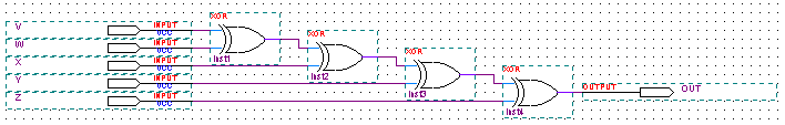
Figure 1: 5-input XOR
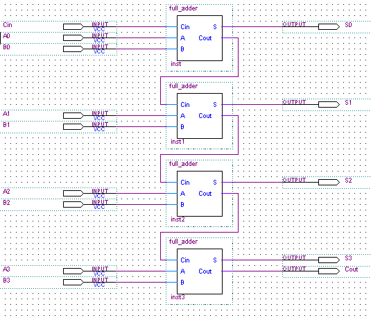
Figure 2: 4-bit adder
You will be creating two different Quartus projects, one for the five-input XOR, and one with the ripple-carry adder. You will then examine the propagation delay of the circuit using both a simple abstract model and then using the Quartus tools to provide a "real" model of the FPGA delay. For the 5-input XOR gate you are to use switches SW0-SW4 (in any order) as your inputs and LEDR[0] as the output.
For the adder SW[3:0] will be "A[3:0]" (in that order), SW[7:4] will B[3:0] (again in that order) and Cin will be KEY3 (recall that the KEY inputs are active low). KEY3 will apply a logical 1 when it is not pushed and a logical low when it is pushed. Your outputs will have S[3:0] mapped to LEDR[3:0] and Cout mapped to LEDG[7].
Implementation details
The 5-input XOR gate should be straightforward to implement. The XOR
gates
needed are found on the symbol tool under "primitives →
logic". The ripple-carry adder requires you to learn a few more
things
about the Quartus tools, so we will step you through it.
Don't forget to save the project early and often!
Once you've finished copying the 5-input XOR design, you will need to do the following to get the 4-bit adder working:
- First, don't forget you want to to start a new Quartus project when doing the ripple-carry adder. That is, the adder and the 5-input XOR should be different projects (and ideally different directories). Call the new project (as well as the top-level module) four_bit_adder.
- Once you've created a new project for the adder, the first
thing you should do is create a schematic as shown in Figure 3. Be sure
to name everything the same as we did (though don't worry about
instance numbers).
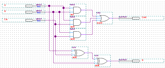
Figure 3: Full-adder
- Save the schematic as "full_adder.bdf" (not four_bit_adder).
- Now select "File
→ Create/Update → Create Symbol files for the current file".
- You will get a message asking you to verify the file, followed
by a
successful completion message.
- Now open a new schematic and name it the same as what you named your top module (You named it four_bit_adder per the above directions, right?). That should be the default when you try to save it.
- When you open the symbol tool, a new option appears "Project".
See Figure 4. Select "Project → full_adder" from the
symbol
tool menu and place the full-adder in your schematic.
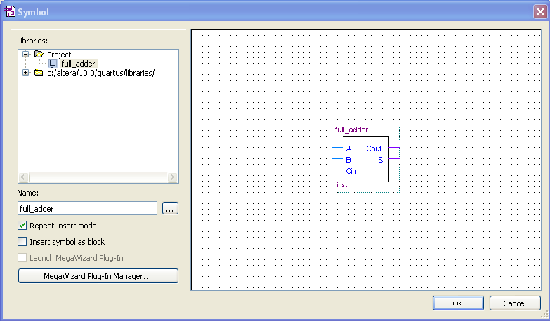
Figure 4: New option in the symbol tool.
- This would be a good time to save!
- Now the full-adder symbol probably doesn't have the inputs and outputs in the same order as they are in Figure 2. So what you need to do right-click on the full_adder symbol and select "Edit Selected Symbol".
- You should find that by grabbing the wires (not the text!) with the mouse, you can change the order of the signals. Make it match what you see in Figure 2 (Cin on the top left, then A then B. On the right you have S on the top then Cout.) Try to keep the spacing about the same as it was.
- Save the file (use the default name which should full_adder.bsf) then close the file ("File → Close").
- Again, this would be a good time to save.
- Now back in the top-level file you will notice that the order of the adder's inputs and outputs haven't changed. Select the adder, right click on it, and then choose "Update symbol or block". That pops up a window asking what you want to update. In this case it doesn't matter which of the options you select (the default is fine).
- Now all you need to do is complete the connections to make your figure look like Figure 2. Be sure to name everything correctly!
- A symbol and project CANNOT share the same name. For example,
you
cannot have a project named fulladder and a symbol named fulladder.
- Generally, you should not start any name with a numeral. Use
Four_bit_adder or adder4bit instead of 4bit_adder.
- Generally, do not name projects or symbols the names of primitives such as AND, OR etc.
- Quartus is not very forgiving with regard to these naming
pitfalls. It will not generate warnings or errors so beware!
- Design Notes and Hints
- Don't forget to save often. Especially when playing with the schematic editor, the software will occasionally crash.
- When you want to run wires from one place to another, you can't generally just drag the wires from start to finish and expect it to look good. You will often need to draw the wire "part way" and then start it from there.
- Functional Simulation: A functional simulation does not model any delay (propagation delay) through the logic circuit. The outputs change instantaneously with the inputs. To set ModelSim for functional simulation, under Assignments → Settings EDA Tool Settings → Simulation → More EDA Netlist Writer Settings set "Generate netlist for functional simulation only" to ON.
- Timing Simulation: A
timing simulation models the delays through the various logic gates.
The
output will not change instantaneously with the inputs. To set ModelSim
for timing simulation, under Assignments → Settings EDA Tool
Settings → Simulation → More EDA Netlist Writer
Settings set "Generate netlist for functional simulation only"
to OFF.
- Deliverables
- Pre-Lab (30 points)
0 0 0 0 0
0 0 0 0 1
0 0 0 1 0
0 0 1 0 0
0 1 0 0 0
1 0 0 0 0
2) Create a test bench and simulation waveform for the 4-Bit Carry Adder that tests the listed input cases. Use the ModelSim setup for FUNCTIONAL simulation (like the tutorial and lab 1). Use a 10ns delay between test cases. Your outputs should include the S0, S1, S2, S3 and COUT. Be sure that the simulation display includes all cases with input and output names clearly displayed. (15 points)
0 1 1 1 1 1 1 1 1
1 0 0 0 0 0 0 0 0
0 1 0 1 0 1 0 1 0
1 1 0 1 0 1 0 1 0
- In-Lab (15 points)
- Post-Lab (30 points)
We will use ModelSim to find the maximum propagation delay of the XOR and the 4 bit carry adder circuits. The maximum propagation delay is the longest time it takes an output to change after a change in the input. Test scenarios to do this are provided for you for each circuit. To measure the delay, you will need to use Modelsim as you did before, but set "Generate netlist for functional simulation only" to OFF (see the Design Notes and Hints). In timing simulation mode, ModelSim will model actual delays on the FPGA.
When running a timing simulation, you will be prompted to choose a timing model. If you do not receive this prompt, you are running a functional simulation, not a timing simulation. The Fast Model runs the simulation using the FPGA's best-case timing delays, and the Slow Model uses the FPGA's worst-case timing delays. If your design works correctly in a Slow Model timing simulation, it is an almost certain indication that the design will work correctly on the actual hardware as well. Therefore, for this lab, and in all future timing simulations in this course, you should use the Slow Model. With the slow model, you will also have to choose either the Slow -7 1.2V 85 Model or Slow -7 1.2V 0 Model. Choose the Slow -7 1.2V 85 Model.