EECS 270: Calculator Lab 

Designing combinational circuits 

See the lab schedule for due dates.
Value: 150 points
v10/8/13

  1. Overview
  2. In this experiment you will learn more about modular design of combinational circuits. The type of circuit you'll be designing lends itself very naturally to this style of design: it is a datapath whose structure, or architecture, is typically determined by the types of operations it is required to perform. In addition, datapath circuit signals come in two distinct varieties: data and control. Control signals determine where to send, or route, the data signals and what operations to perform on them. Data signals, on the other hand, are the primary carriers of information in the circuit, and are typically bundled as multi-bit words. Datapath circuits tend to be quite regular, allowing the use of a structured design approach that simplifies the design process and leads to easily testable implementations.

  3. Preparation

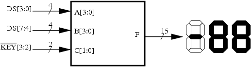
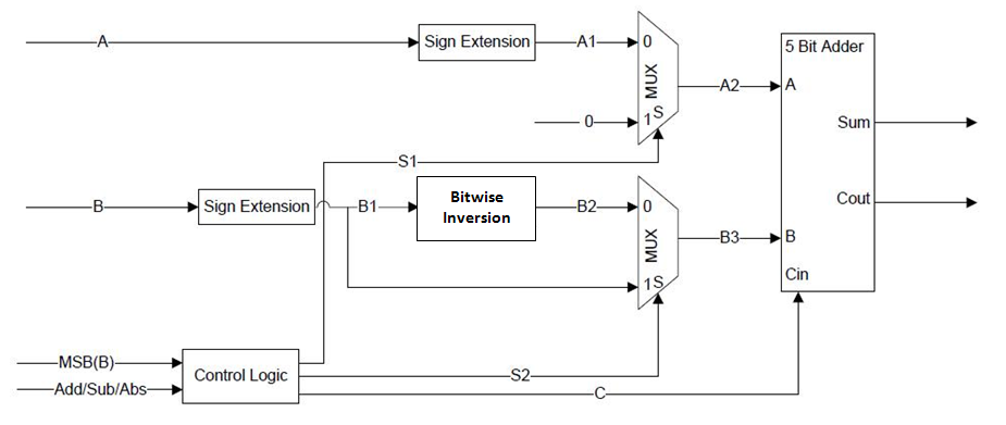
  4. Figure 1: Top-level view of the CALCULATOR circuit.

  5. Design Specification
  6. The top-level schematic of the CALCULATOR circuit is shown in Figure 1. It has a 2-bit opcode C and two 4-bit operands A and B that represent two's complement integers. The output F must be generated according to the following function table:
    Key3 (C1) Key2 (C0) Operation
    Pressed Pressed Display A+B
    Pressed Unpressed Display A-B
    Unpressed Pressed Display the absolute value of B
    Unpressed Unpressed Display the absolute value of A
    Table 1: Calculator operations
    The A and B operands should be connected, respectively, to DIP switches 3-0 and 7-4 (the higher number being the MSB). The opcode bits (C[1:0]) should be controlled by the two leftmost buttons. The CALCULATOR output (F) should be displayed in decimal signed-magnitude notation using three 7-segment LEDs: The two rightmost to display the 2-digit decimal magnitude, and the next one (on the left) to display a negative sign for negative results (the middle horizontal bar).

    Restrictions

    1. The top level module may be in schematic or Verilog.
    2. Sub modules may be in schematic or Verilog.
    3. You may use any Verilog constructs you learned thru  lab  3.
    4. You can use the conditional ? operator. Look in the Verilog combinational reference or slides for details. It is a very powerful way to implement an N-bit, 2 to 1 multiplexer.
    5. You CANNOT  use the "+" or "-" Verilog operator. This will greatly simply the design.
    6. You may only use one n-bit ripple carry adder!! This will be strictly enforced. You can use the schematic editor version implemented in lab 2 or write it one in Verilog. Of course, you cannot use the + or - Verilog operator.
    7. Your design should use combinational blocks that implement such functions as: ones complement, sign extension, MUXs and data path control.
    8. The inputs A and B must be expressed as buses, ie A[3..0] and B[3..0]. See the accompanying guide on using buses for schematic entry.

  7. Design Notes and Hints
                        module _4bit2to1mux(A, B, S, C);
                        input [3:0] A, B;
                        input S;
                        output [3:0] C;

                        assign C = (S = = 1) ?  B : A;
                        endmodule

                    Or this is equivalent to

                             if (S = = 1) C = B;
                            else C = A;

  1. Deliverables
  2. Pre-Lab (55 Points)
1) What is the range of positive and negative input values? Give your answer in decimal. (5 points)
2) What is the range of possible positive and negative output values given the above input values? Give your answer in decimal. (5 points)
3) Using both 4-bit and 5-bit two's complement representation, express the numbers 4, -4, 6 and -6. (5 points)

4) The following block diagram illustrates the connections and functional components (combinational blocks) to implement a partial calculator. This is a starting point. You will have to add more components to complete the In-Lab. Complete the table that follows for each case. The first case is completed as an example. All values are in binary and should be completed in binary. dc means don't care. Input values are to be interpreted as 2's complement. 5 points for each case.


Operation A  A A1      S1 A2 B B B1 B2 S2 B3 C Sum
Binary
Sum
Signed Decimal
A + B 0001 1 00001 0 00001 0010 2 00010 11101 1 00010 0 00011 3
A + B 0011 3 . . . 1111 -1 . . . . . . .
A + B 1011 -5 . . . 1110 -2 . . . . . . .
A - B 0001 1 . . . 0010 2 . . . . . . .
A - B 1111 -1 . . . 0001 1 . . . . . . .
| B| dc . . . . 1101 -3 . . . . . . .
|B| dc . . . . 0011 3 . . . . . . .

5) Write a Verilog module that provides the sign extension module. (5 points)

6) Write a Verilog module that provides the ones bitwise inversion. (5 points)


 In-lab (55 points)

    Demonstrate the operation of your final calculator design to the lab GSI. Be sure that the following cases work before demonstrating.

     1 + (-7) = -6
    0 - 7 = -7
    -1 + 1 = 0
    7 - (-8) = 15
    -8 + (- 8) = -16
    |7| = 7
    |-8| = 8
    Post-Lab (40 Points)
    1. Provide schematic and/or verilog  design files depending on your implementation.(10 points)
    2. Provide a functional simulation of your final calculator design for the following scenarios listed below.. The output must be provided directly from the adder, bypassing the 7 segment encoder. Add extra ports to your design to accomplish this. Notice writing all the test cases will be quite tedious with 16 cases per simulation! It is possible to use the for loop operator to generate the 16 test cases. In addition, using bus notation to make your port connections will greatly simplify the connection between the test cases and design module. An example test bench and simulation output for the first simulation case is provided. You must express the input arguments and sum output as a signed decimal number. To do this, in the waveform window, select the bused signals such as A_s, right click, select radix and then decimal.  (10 points each)
      1.  5+(all possible values)
      2.  abs(all possible values) (on B)
      3.  4-(all possible values)

  1. Appendix A: Using ?: to display values to the 7-segment display
  2. A very useful Verilog operation is the ternary (also called "conditional") operator "?:". It works as follows:
    assign bob=(mary==1'b1) ? 2'b01 : 2'b10;
    This is basically the same as saying
    if(mary==1'b1)
    bob=2'b01;
    else
    bob=2'b10;
    This operator can be thought of as a MUX.

    Consider the following coding example (parameter is a way to declare a constant).

    module display(letter,seven);
    input [1:0] letter;
    output [6:0] seven;
    parameter F=7'b1000111;
    parameter S=7'b1011011;
    parameter r=7'b0000101;
    parameter L=7'b0001110;


    assign seven= (letter==2'b00 ? F:
    (letter==2'b01 ? S:
    (letter==2'b10 ? r:
    L)));
    endmodule
    This uses the ?: operator to assign values to the seven-segment display depending upon the value of "letter".

    Important: Quartus appears to occasionally be very sensitive to a lack of spaces around the ? operator.