Paul Piong Sam Berro Dimitri Karatsinides
Light Writer
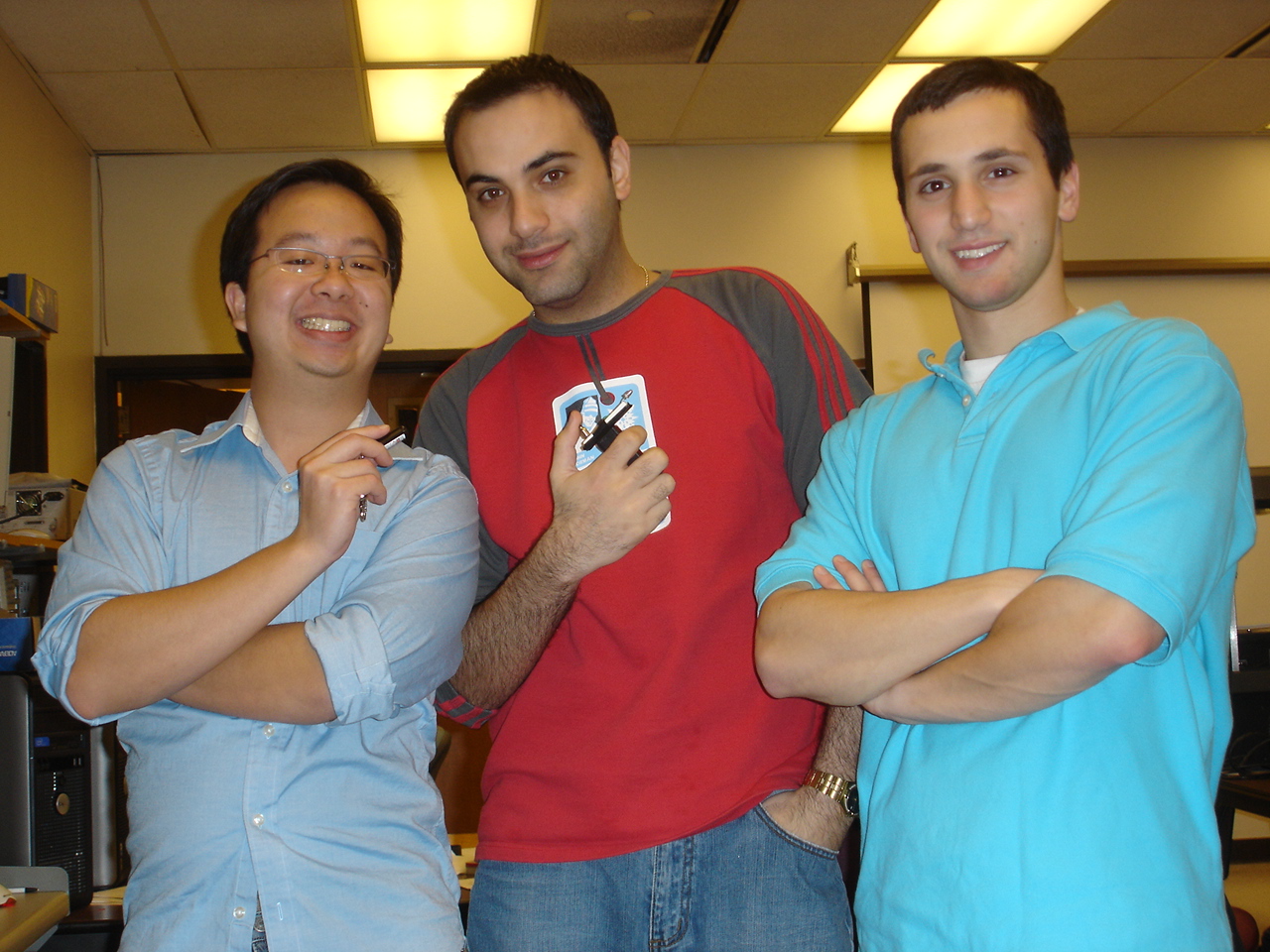
Paul Piong (L), Sam Berro (C), Dimitri Karatsinides (R)
Introduction High Level Design Hardware Software Putting it all Together
Work Distribution Downloadable Videos YouTube Videos Conclusions Special Thanks
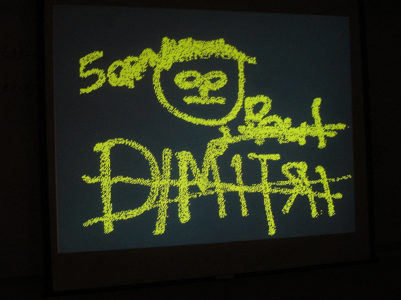
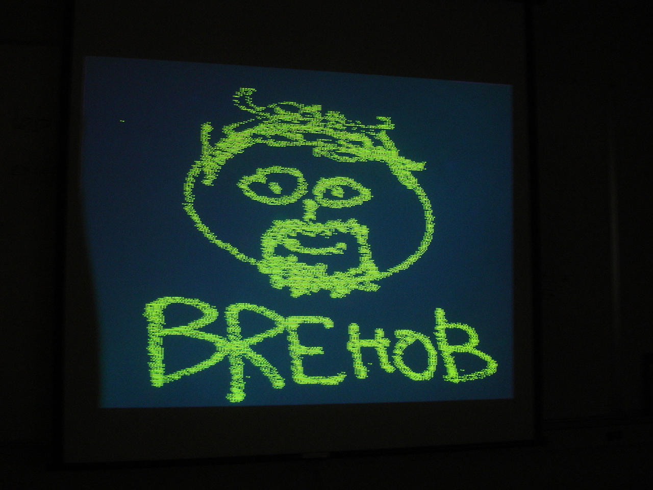
The purpose of this project was to create the ability to "write" on a surface (white wall, projector screen, etc) with a laser pointer. The initial idea was found from a group of graffiti artists who implemented a similar, very large system, to write on the sides of tall buildings. ( http://graffitiresearchlab.com/?page_id=76#video ) Our system has the following characteristics:
Compact: All of the system components fit into a small box
Portable: System can be moved anywhere by a single person
Ease of Use: Controls for the system would be simple enough for anyone to use
Scalability / Upgradeability: System is built to be easily modified and/or upgraded
Fully Embedded: No PC/Laptop required
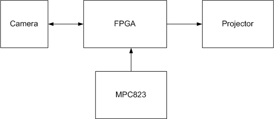
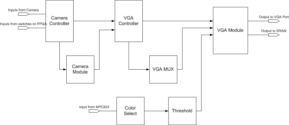
The camera outputs data to the FPGA, which determines if the data is above a threshold value. Also the FPGA has the ability to configure registers on the camera via the bidirectional ports. The FPGA then continuously outputs a VGA frame to the projector (or an LCD monitor) with the path that the laser has drawn, with the color selected by the MPC823.
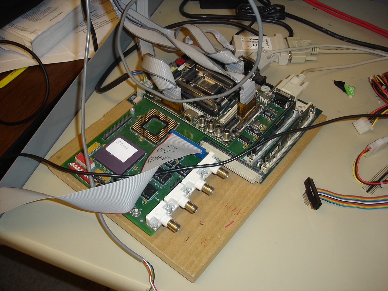
This project was not based on the MPC823 and the lab's Xilinx FPGA. Instead, the system was based on a more powerful, Altera DE2 FPGA. The hardware components and they're uses are listed below:
M4088 Black & White camera: This is what the system uses to "see" where the laser pointer is pointing. This camera has an 8 bit output, 0x00 corresponds to black, 0xFF corresponds to pure white. The laser shows up very close to pure white.

Breakout Breadboard: This board was used as an intermediary device between the camera and the FPGA. This board was necessary to appropriately map pins on the camera to pins on the FPGA. The board was also used to eliminate the risk of sending too much current to/from the FGPA. This was done by inserting resistors in series with all data and other signal pins.
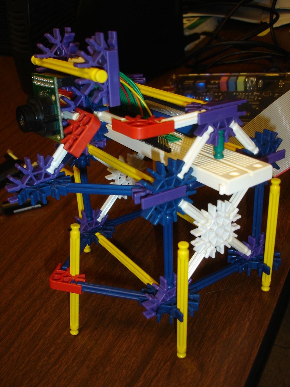
K'NEX Camera Mount: This mount was created to stabilize the camera. This mount houses the camera and the Breakout Breadboard. The mount allows us to manually calibrate the camera with the projector's output.
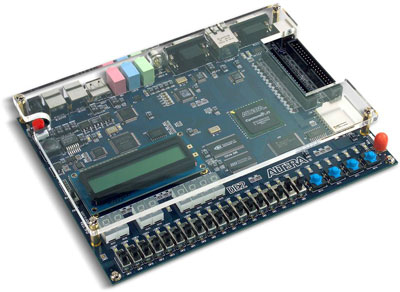
Altera DE2 FGPA: This FPGA is the main component of the whole system. This FPGA was chosen over the Xilinx FPGA that resides in the EECS 373 lab because of its increased capabilities. The DE2 took in clock, sync, and pixel data in from the camera, conducted various operations on the input data, and output the proper display data. The DE2 also has a bank of switches and pushbuttons which are used to control various actions of the system.
PowerPC 823: The PowerPC board was used to control the different colors that the system would output. Hyperterminal is used to communicate to the PowerPC board via an RS-232 serial cable. These commands are sent to the DE2 via the Xilinx FPGA and a data ribbon cable.
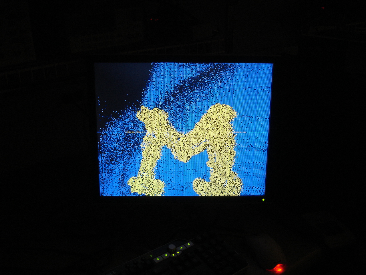
Projector or Computer Monitor: For testing purposes, we used a computer monitor to see the outputs of the system. Once the initial system was up and running, a projector was used to tune the system. The final system uses a projector.
Testing with the Computer Monitor Fine Tuning with the Projector (Paul (L) and Dimitri (R))
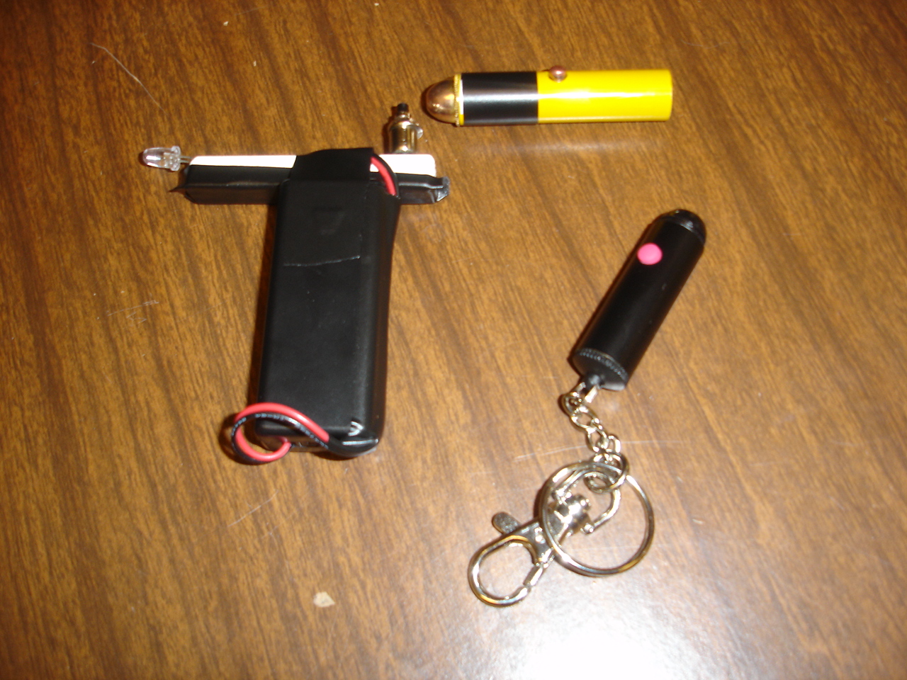
Laser Pointers and Spray Light: These were used to write on the screen. The Spray Light™ imitates a spray paint can. The Spray Light™ was developed using the latest in LED technology.
Spray Light™ (L), Laser Pointers (R)
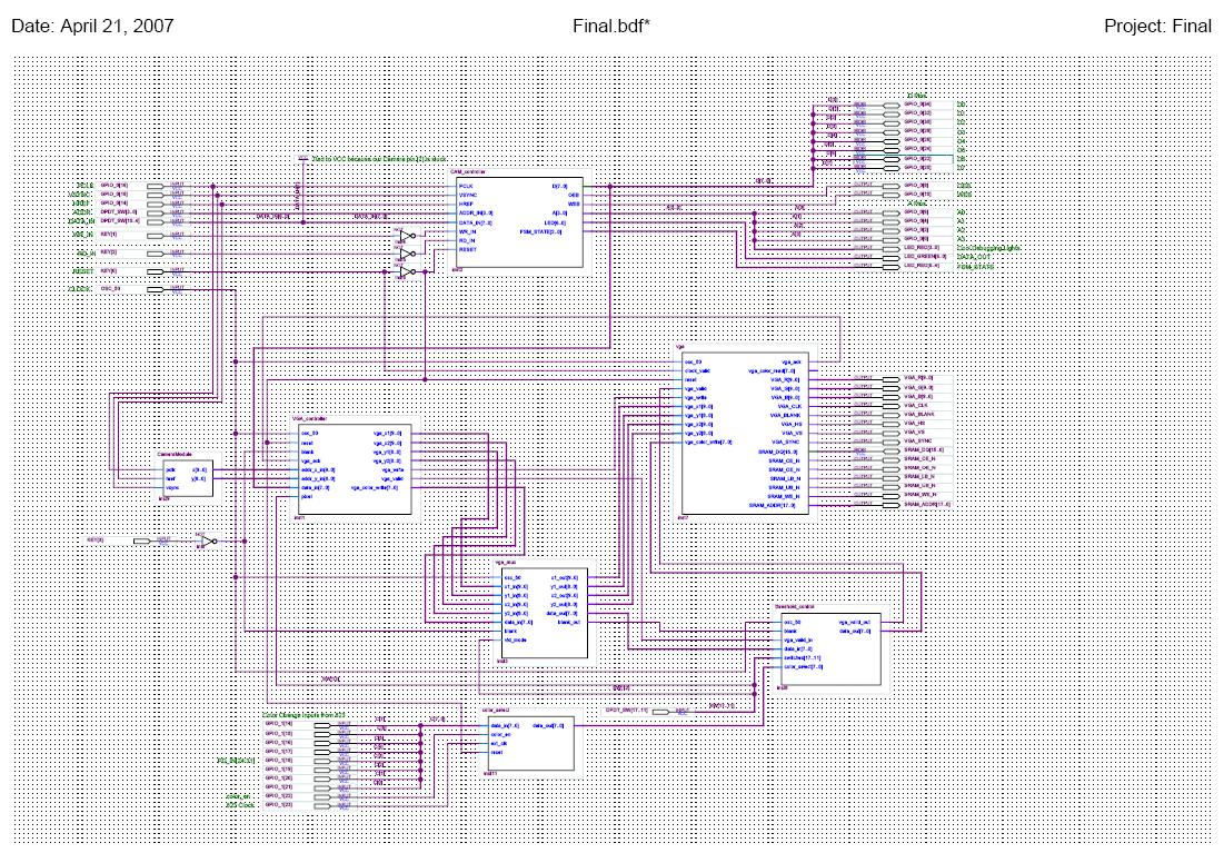
The majority of the software in the system was programmed in Verilog. Certain modules (CameraModule) were programmed using VHDL (yay STD....LogicVector). Each of the components were connected to eachother using schematic capture. Shown below is the top-level schematic view of the system as well as a brief description of the the individual components.
Top Level Views
Inputs:
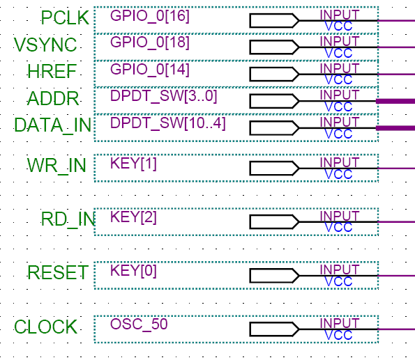  |
PCLK: Pixel
clock from camera. A new pixel would arrive at this 7.14MHz rate VSYNC: New Frame Signal. Between every frame, VSYNC gets asserted HREF: Asserted High while camera outputs an entire, horizontal line. Goes low in-between horizontal lines ADDR: 4 bit address bus to control registers on the camera. Takes switches as inputs. DATA_IN: 8 bit value (from FPGA's DIP switches) to be written address on camera specified by ADDR. WR_IN: Pushbutton input from FGPA to write data to camera RD_IN: Pushbutton input from FPGA to read data from camera RESET: Pushbutton input from FPGA to reset all internal systems CLOCK: 50MHz system clock BLANK: Pushbutton input from FPGA to "blank out" the screen. (Makes screen go black) MISC: Miscellaneous switches. Uses include threshold control, writing color (for the laser), etc. |
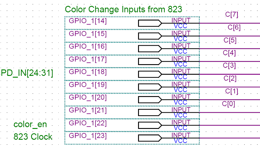 |
data_in[7..0]:
Color code from the MPC823 entered via hyperterminal color_en: enables the color latches in the color module. New color is acquired when high ext_clk: 50MHz clock from the MPC823. reset: Reset initialize signal. |
Outputs:
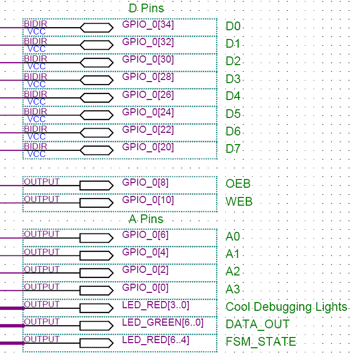 |
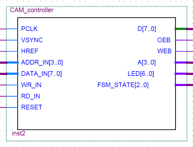
CAM_controller pin
descriptions D Pins: 8 bits of bi-directional data to the actual M3088 camera module. These are connected through the GPIO_0 bank on the FPGA and either read or write data based on the control signals from the CAM_controller module OEB: Output Enable Bar, one of 3 control signals to the M3088 camera. This signal is active low and controls the tristate for the bidirectional pins on the camera. WEB: Write Enable Bar, another control signal to the M3088 camera. This signal is also active low and tells the camera when a write is to be performed based on the address and data to the camera. The last control signal CSB (Chip Select Bar) is always held low since we only have one device. A Pins: 4 bits of output to the camera which decide which register to read from or write to. Debugging LEDs: The 8 Green LEDs show the pixel data coming from the camera and generally just show us that the camera is functioning. It also allows us to verify the value we write to the registers on the camera. The Red LEDs keep track of the states used in the finite state machine and general |
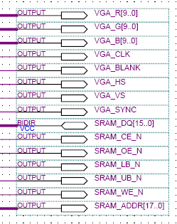 |
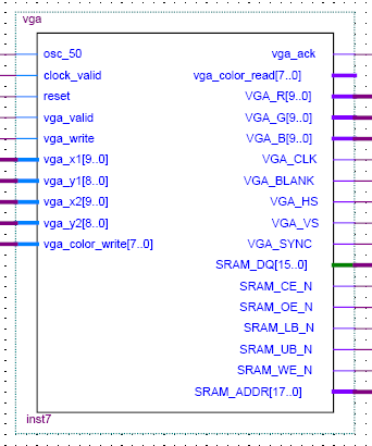
VGA_R, VGA_G,
VGA_B: Output pins to the VGA decoder on the DE2 board. These signal
the pixel color to be displayed. VGA_CLK: Output to the VGA decoder on the DE2 board. This clock is generated to produce a 60 Hz display. VGA_BLANK: Output to the VGA decoder on the DE2 board. This output tells the decoder when to blank the screen if required. VGA_HS, VGA_VS: Output to the VGA decoder on the DE2 board These signals control the Horizontal and Vertical Sync pulses and are generated along with VGA_CLK to give a 60Hz output. VGA_SYNC: Output to the VGA decoder on the DE2 board. This is a signal the decoder needs to synchronize with the controller. SRAM_DQ: Bidirectional ports to the SRAM. These pins serve as both read and write ports to the SRAM on the DE2 board. SRAM_CE_N, _OE_N, _WE_N: These are standard control signals to the SRAM on the DE2 board, and are active low. SRAM_LB_N, SRAM_UB_N: These signals tell the SRAM to write to either the high or low bytes. SRAM_ADDR: These are control signals that specify the address of the location to be written to the SRAM on the DE2 board. |
CAM_controller:
 |
CAM_Controller is the module that controls the camera. It asserts
the proper signals to the camera to get the camera to operate properly.
All inputs from the camera and all outputs to the camera are routed
through this module. This module contains a finite state machine
and is written in Verilog.
|
CameraModule:
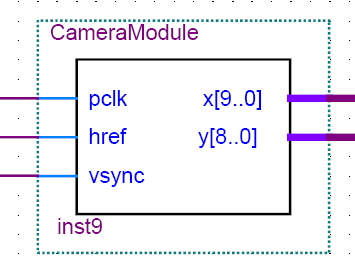 |
CameraModule is the module that keeps track of what pixel the camera is outputting. The three inputs (pclk, href, vsync) indicated each pixel, horizontal row, and frame respectively. From these inputs, a series of counters are used to generate x and y position on the screen. Functionality exists within this VHDL module to expand the camera's 384 x 288 image to fit the 640 x 480 resolution of the PC monitor or the Projector. |
color_select:
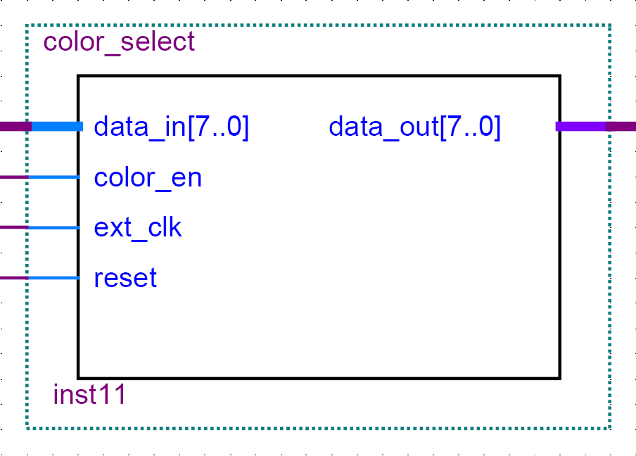 |
color_select module is the module that interfaces with the PowerPC823.
This Verilog module reads in the color codes sent from the PowerPC board
(8-bit codes) and holds that color value on data_out. This color
stays on data_out until a new color is sent from the PowerPC. This
is done using a finite stat machine that changes the output on the
assertion of color_en.
|
vga_mux:
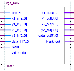 |
The
vga_mux module uses the "blank" signal to select whether pass the camera
outputs to be thresholded and displayed, or (on "blank" high) pass a
blank screen. This module also puts a fixed square in the top left part
of the display which blanks the screen when the laser pointer passes
over.
The "vid_mode[1]" signal
prevents the top left region from blanking the display when written to
for the purpose of displaying live camera feed on the whole screen.
|
VGA_controller:
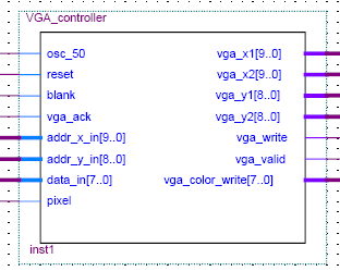 |
VGA_controller takes in the address generated by the camera as well as
the data and runs through a finite state machine. This generates control signals that tell the VGA module when to latch the data in. These signals were generated to mimic the transaction signals that the E100 processor used in EECS 100, since we were using it as a dedicated device. Additionally, if we are in double pixel mode this gives the VGA module (x1, y1) (x2, y2) addresses that increase the pixel size to be 2x2.
|
Threshold_control
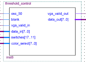 |
The "Threshold_control"
module is responsible for detecting and passing the coordinates of the
laser pointer dot to the "vga" module to be displayed. This is done by
comparing the brightness of the "data_in[7..0]" to a threshold value.
This value is set by switches [17..11]. These switches also provide a
live feed real mode display fo the camera input. The color data passed
to the "vga" module is controlled by the "color_select" input signal and
"blank" signal. When in threshold mode, the module asserts a vga_valid signal if the threshold is met and pixel data coming in is valid. This enables writing that pixel coordinates to the screen using the color specified in the color register inside the module.
|
VGA
 |
This VGA module was supplied by
ENGR
100 Section 700 (Microprocessors and Music: An
|
In the initial phases of the project, we wanted to run this system on the MPC823 / Xilinx setup. This was ruled out due to a lack of capabilities on the Xilinx board. We decided to use the Altera DE2 FPGA since it has improved memory, a greater number of logic units, and more DIP switches and pushbuttons. All the modules in the project were developed by the team with the exception of VGA.v, which was created by Prof. Chen of ENGR 100.
Much discussion and brainstorming was attributed to the difference in clock domains between the VGA and the camera. The camera has its own pixel clock (7.14MHz) and the VGA operated on the FGPA system clock (50MHz). Overcoming this issue was the largest challenge of the project. Initially, we were going to create a buffer that stored the addresses of the pixels that were greater than the threshold value. A handshake system was to be created to tell the camera when to take a frame, and when the VGA could read in new data. After extensive attempts, this idea was turned down due to its complexity and time contraints.
Since the VGA takes in a pixel address, we decided to directly send pixel data and addresses from the camera to the VGA. This was somewhat successful, although the images we viewed were not entirely stable. Stability issues were fixed when we found bugs in our pixel address generator (CameraModule.vhd) and when addresses were latched into VGA_Controller (previously were not latched into the module).
Once these major tasks were completed, the thresholding capabilities were added using vga_mux.v and Threshold_control.v. vga_mux gives the capability to "blank" the screen, i.e. turn the screen black. Also, the ability to blank the display by pointing at the top-left corner of the viewing surface was added in this module. Thresholding the individual pixels was done in Threshold_control.v. Here, if a pixel exceeds the threshold value, the selected writing color will be written to that pixel in memory. If not, the vga_valid signal will be de-asserted and SRAM will not be changed.
Lastly, the ability to change the desired writing color was added. This was implemented using the PowerPC823 and Xilinx FGPA board in Lab. We added this functionality mainly because the DE2 ran out of DIP switches. Using hyperterminal, the user inputs an 8 bit color code which is transmitted via an RS-232 cable to the PowerPC. From here, the data goes to the Xilinx FPGA, and then to the Altera DE2 via a 40-pins IDE cable.
Paul: Initial Idea, Camera Interface, Altera2 guru
Sam: Verilog Guru, blanking specialist
Dimitri: K'NEX guru (also likes VHDL)
Project Light Writer
Color Test
Pacman
LSA student
I Wish...
http://www.youtube.com/watch?v=e1RmSnnEIQY
Initial Build
http://www.youtube.com/watch?v=zHYKAgM_VGY
Go Blue!
http://www.youtube.com/watch?v=n5c_CS9CWY4
This was a really fun project to do, although it did take more time than expected. The results were very very 0xC001, and the response of the system was excellent. During the course of the project however, the 8th data pin on the camera was stuck on high and as a result we could not turn the auto exposure mode off. This meant that use of the system in anything but a sufficiently dark room was not possible as too much stray light would affect the threshold output (as we found out on demo day!).
Further improvements to the project would be to allow color palettes on the display to select colors on screen with the pointer. Also it would be nice to have a software method of aligning the laser with the output automatically, or having a platform that adjusts itself.
Professor Mark Brehob
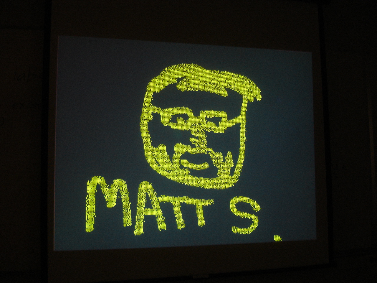
Matt Smith
Professor Peter Chen
Professor Kurt Metzger