EECS 373 Lab 1: Introduction to the Hardware Development Tools
Schedule
See posted lab schedule for due dates, in-lab, and post-lab due dates.
Objectives
In this lab you will learn to:
- Use Microsemi's integrated design environment (Libero SoC) to
implement a simple logic function in the FPGA hardware.
- Observe logic signals with a simple low cost analyzer Logic
Analyzer, a high end Logic Analyzer and Oscilloscope.
This lab reference guide "Libero Project Flow Reference Guide" is quite
lengthy because of the many screen shots and
detailed procedures. This is a necessary introductory phase to get you
acquainted hardware development tools. While the document is long, you
should be
able to finish the In-lab section within the lab period. You may also
get a
good start on the Post Lab assignment, but will likely have to finish
outside the lab period. You will be given 24 hours access to the lab
the
first lab period via keypad entry so that you may use the lab at your
convenience. There will also be additional supported open hours that
will
be posted on the course web page.
Pre-Lab Assignment
There is no Pre-Lab assignment for this lab. The lab requires no
preparation. Consider reading over the Libero SoC tool flow tutorial.
You will spend most of your in lab time doing this exercise.
In-Lab
Do the Libero Tutorial
posted with the lab. Be sure to do all the parts. It
will provide you with everything
you need to do the post lab. Don't hesitate to get started on the post
lab once you are finished with the tutorial and basic instrument
review.
Post-Lab
You may (should) work with your partner for the Post Lab. Only one
submission for each assignment is necessary. The assignment is due
within the first hour of your next home lab section.
The demonstration can be made during any staffed lab before the
deadline. All other materials should can be submitted via Ctools before
the deadline.
Post-Lab assignment 1: Hardware Design
Design and Implement hardware using Verilog and the 100 Mhz system
clock that will sequentially blink LEDs 0 - 7 back and forth. See example video.
Each LED should only be on for 0.25 seconds.
Hints:
1) Be sure and read over the common pitfalls section at the end of the
Libero Tutorial.
2) Don't forget to check the synthesis warning by opening Synplify as
shown in the Libero Tutorial. Some warning such as implied latches will
keep your design from working.
3) Consider just blinking one LED to start to make sure your counter is
working.
Print the demonstration sheet and have
one of the lab staff verify the functionality of your hardware. Be sure
everyone in your group is included on the demonstration sheet. The lab
instructor will collect the demonstration sheet at this time.
Post-Lab Assignment 2: Digital Signal Observation
Probe one of the LEDs with the Saleae and verify the on
time.
Submit a screen shot including the period measurement.
Probing
LED 0
Reference the Basic Lab Equipment Introduction for specific information
on how to use the instruments. The Saleae logic analyzers are not
included with your kits or the stations. You will have to get one from
the lab instructor.
Submit a screen shot with your post
lab.
Post Lab Assignment 3: Observing Switch Bounce
Observe the switch bounce for one of the push button switches on your
kit with the oscilloscope. Reference the Libero tutorial to probe the
switch and the Introduction to the Lab Equipment for information on
triggering the scope. Safe a screen shot of the scope to a USB drive
and submit it with your post lab.
Submit a screen shot of the
switch bounce with your post lab.
Accessing the Lab and Support outside of your Home Lab Period
Typically, you will not be able to complete your lab during the home
lab time. Most labs can take 2 to 4 times the duration of one home lab
period. You may attend the other home lab periods if there is room.
Home lab students have priority during their home lab period.
Alternatively, there are several open supported labs provide through
out the week. See the supported hours schedule posted on the home lab
web page for times. You may attend any open lab.
In addition, you may use the lab anytime there is not a scheduled
conflict.You will be given a keypad entry code to the lab so you can
use the
lab
any time other lab sections are not meeting. Be sure and read
the
unsupported lab policy before using the lab. There are important lab
safety
issues documented in the policy.
References
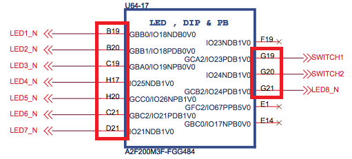
LED, SWITCH, USER I/O Pin-out
Quick Reference
Here are the pin numbers of the
SmartFusion chip that are connected
to the physical LED1-8, SW1,2 and user IO 1-5. The figures are specific
to the kit and can be found in the kit reference manual. http://www.actel.com/documents/A2F_EVAL_KIT_UG.pdf.
Note, the LED numbering in the following figure begins with one.
LED
and Pushbutton Switch FPGA Pin Numbers