This lab will introduce you to the hardware prototyping board (DE2-115) and computer-aided design software (Quartus) you will use this semester. The lab will walk you through the steps needed to implement, download, and test a simple digital circuit.
You will build several digital circuits this semester, ranging in complexity from a simple function of inputs to a general-purpose computer. Altera's DE2-115 board is the vehicle you will use to implement these circuits.
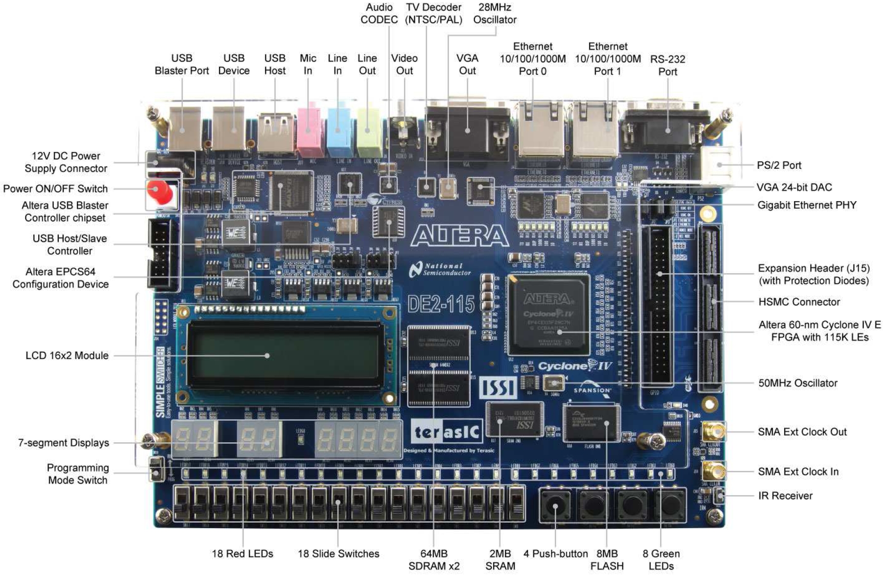
| The DE2-115 (shown on the right; click to expand) is designed to support a wide range of experiments. It combines a variety of logic and I/O devices onto a single printed-circuit board and allows you to configure and control these devices to create different applications. The logic devices on the DE2-115 are an FPGA (a programmable logic device) and several memory components (SDRAM, SRAM, and flash RAM). The I/O devices on the DE2-115 are a small LCD display, numerous LEDs (lights), and switches. In addition, the DE2-115 has connections to a variety of external I/O devices, including PS/2 keyboard, USB mouse, VGA monitor, camera, microphone, speaker, Ethernet, RS-232 (serial port), Secure Digital card and IrDA (infrared). |
|
In this first lab, we will use the Cyclone IV FPGA, LEDs and switches.
This lab will walk you through each step of the design process. Altera provides a similar tutorial, but you don't need to read it unless you're curious.
Quartus calls a digital circuit a project. All files for a Quartus project will be stored in one directory. To create a new digital circuit, first create a new directory to hold all information for the digital circuit. The directory may be named arbitrarily; these instructions assume your directory is named lab1. Create this directory somewhere under your ITCS AFS home directory.
Next, start Quartus by opening a terminal window and typing quartus (see Using computers in ENGR 100 for how to open a terminal window). When Quartus starts, it will offer you the choice to create a new project or open an existing project (screenshot). Click Create a New Project (New Project Wizard). If Quartus does not ask you this automatically, you can invoke the New Project Wizard through the File menu (File -> New Project Wizard) (screenshot). (We use the convention Menu1 -> Menu2 -> Item to describe how to click through a series of menus. All mouse clicks are assumed to be with the left mouse button, unless otherwise specified.) Here is a screenshot of the first window displayed by the New Project Wizard. Click Next to skip this introduction.
Fill in the dialogue boxes on the next window of the New Project Wizard (screenshot). The working directory for this project is the directory you created, e.g., lab1. You can specify the directory by clicking the ... icon, navigating to the directory, and clicking Open. We suggest you name your project top. The top-level design entity for all projects in this class must be top. Click Finish to end the New Project Wizard (there are subsequent dialogue boxes, but we won't need them for this lab).
At this point, you've created a Quartus project file top.qpf in the lab1 directory. You can open this project later within Quartus via File -> Open Project, navigating to the project directory, and selecting top.qpf (screenshot 1) (screenshot 2).
After the New Project Wizard completes, you must configure the project for the DE2-115. To do this:
Now that you've created a Quartus project, it's time to enter your first digital circuit. All circuits in the class will be expressed in Verilog code. You can use Quartus's built-in text editor (or any other text editor) to edit Verilog code. Do not use a word processor such as Microsoft Word or OpenOffice, since word processors include extraneous formatting information in their files.
Quartus' text editor can be invoked through Quartus' File menu (File -> New -> Design Files -> Verilog HDL File) (screenshot 1) (screenshot 2).
Use the text editor to enter the following Verilog code (screenshot), which implements a "majority vote": the output of the LED will be 1 if and only if two or more of the switches are 1.
    module top(
        input wire [17:0] SW,
        output reg [17:0] LED_RED);

        always @* begin

            LED_RED[0] = 1'b0;      // default value is 0

            case (SW[2:0])

                3'b011: begin
                    LED_RED[0] = 1'b1;
                end

                3'b101: begin
                    LED_RED[0] = 1'b1;
                end

                3'b110: begin
                    LED_RED[0] = 1'b1;
                end

                3'b111: begin
                    LED_RED[0] = 1'b1;
                end

            endcase
        end
    endmodule
Save the code as top.v (File -> Save As) (screenshot 1) (screenshot 2). Make sure the box is checked to add this file automatically to the current project.
A few points about the Verilog code above:
We'll learn more about Verilog as the semester progresses. Surprisingly, there are only a couple more Verilog constructs you'll need to describe all possible circuits. The labs will teach all the Verilog you'll need; if you want more comprehensive information on Verilog, see Deepak Kumar Tala's tutorial or Stuart Sutherland's reference manual.
The next step is to translate the high-level hardware description written in Verilog to a low-level circuit specification for the FPGA. This step is called synthesis (Quartus calls it compilation). You can invoke Quartus' compiler through the Processing menu (Processing -> Start Compilation) (screenshot) or a keyboard shortcut (Ctrl-L). Later in the semester, we will describe how Verilog constructs are synthesized to digital logic.
Quartus displays the status of the compilation as it runs (screenshot). The small Status window on the left shows the progress of each phase of the compilation. The wide window at the bottom displays compilation messages, including warnings and errors. Quartus will notify you with a confirmation box after it finishes compiling your circuit. It will issue numerous warnings about unused signals and I/O assignments. You can ignore most of these warnings, but you should look through them in this lab to familiarize yourself with the standard warnings. In later labs, you will be able to debug a lot of problems (and save a lot of time) by looking for unusual warnings. After you click OK, you'll get the following screenshot.
If the compiler encounters an error (e.g., you had a typo), the bottom window will show an error message that is usually helpful for diagnosing the cause of the error (screenshot). Double-clicking on the error message will usually open the file with the offending code (screenshot). You can then fix the error and re-compile.
After you've compiled the Verilog code, you're ready to download it onto the Cyclone IV FPGA. Quartus downloads the synthesized circuit to the FPGA via the USB cable that connects the DE2-115 to the computer that is running Quartus.
First, turn on the DE2-115 (if it's not already on) by pressing the power button (big red button on the upper left). This should light up the blue power LED (upper left).
You will download the synthesized circuit via Quartus' In-System Memory Content Editor (which we call the "memory editor" for short). Start the memory editor from Quartus' Tools menu (Tools -> In-System Memory Content Editor) (screenshot). You will see the following screenshot.
The only part of the memory editor we will use for this lab is the top, right-hand corner of the memory editor (JTAG Chain Configuration). Drag the vertical divider (just to the left of "JTAG Chain Configuration") to the left so you can see more of that part of the memory editor. Click the Hardware pulldown menu and select USB-Blaster (screenshot). If no options appear, wait 45 seconds and click the Setup button to the right, then select USB-Blaster (Quartus needs some time to recognize the board).
Now click the ... button, which will bring up a window to select the programming file (screenshot). Navigate to the project directory and select top.sof; this file contains the low-level circuit specification you created when you compiled the Verilog code.
Finally, click the blue arrow icon. This downloads the circuit onto the FPGA. Quartus may pause for about 30 seconds the first time you download a circuit; subsequent times will be much faster.
Now that you've entered, compiled and downloaded your circuit, it's time to test your circuit's behavior. The switches used in this circuit are SW[2], SW[1], and SW[0] (labeled SW2, SW1, and SW0 on the board). Move the levers of these switches between 0 (closer to the front edge of the DE2-115) and 1 (away from the front edge of the DE2-115) and observe the output of LED_RED[0] (the LED directly above SW[0]).
Does your circuit behave as expected? If so, congratulations! You've implemented your first digital circuit. If not, edit top.v and fix any mistakes you made when entering the code.
Another way to express this circuit is with Verilog's "if ... else if" statement. The following code implements the same circuit as the code above. Comment out the case statement in your code, replace it with the "if ... else if" statement below, and verify that it also implements a majority vote.
    module top(
        input wire [17:0] SW,
        output reg [17:0] LED_RED);

        always @* begin
            LED_RED[0] = 1'b0;        // default value is 0

            if (SW[0] == 1'b1 && SW[1] == 1'b1) begin
                LED_RED[0] = 1'b1;

            end else if (SW[0] == 1'b1 && SW[2] == 1'b1) begin
                LED_RED[0] = 1'b1;

            end else if (SW[1] == 1'b1 && SW[2] == 1'b1) begin
                LED_RED[0] = 1'b1;

            end
        end
    endmodule
A few points about the Verilog code above:
Now that you've implemented a digital circuit, experiment a little to see if you can implement some other simple functions. You can do this within the same Quartus project or in another Quartus project (which would be stored in a separate directory).
Try implementing a circuit that compares two unsigned 4-bit numbers. Each number will be represented in binary by the values of 4 switches. Refer to the first number as SW[7:4] and the second number as SW[3:0]. Verilog operators interpret multi-bit values as unsigned numbers, so you can express this circuit in only a few lines of Verilog, using an if statement. Write, enter, download, and test Verilog code to light an LED when the value of SW[7:4] is greater than the value of SW[3:0].
Now try implementing a circuit that subtracts one 4-bit number from another, producing a 4-bit output. The numbers can again be input through the switches, i.e. SW[7:4] and SW[3:0]. Just as you input a 4-bit number using Verilog's array notation (SW[3:0]), you can output a 4-bit number using the same notation (LED_RED[3:0] = some value). Again, you can use Verilog operators on multi-bit values, so your code should be very short (hint: this circuit won't have an if statement). Don't worry about inputs that produce negative results.
Each lab will include tasks for you to do to prepare for your lab section. You should complete these tasks before your lab meets. It will be difficult for you to complete the lab during your lab section if you do not complete the pre-lab assignment before your lab meets.
Your pre-lab assignment for this lab is to read through this handout.
After you have demonstrated one of the two variations to a lab instructor, submit the top.v you demonstrated.