Overview Research Teaching Publications Personal
Address:
4765 BBB Building, 2260 Hayward Avenue, Ann Arbor MI 48109-2121, USA Tel: +1 (734) 763-2107 Fax: +1 (734) 763-8094 e-mail: pinakimazum AT gmail DOT com Professor Pinaki Mazumder received his Ph.D. in Electrical and Computer Engineering from the University of Illinois at Urbana-Champaign and then joined the Department of Electrical Engineering and Computer Science at The University of Michigan where he has been teaching for the past 25 years. He worked for 6 years in industrial R&D laboratories and spent his sabbatical year at University of California at Berkeley, Stanford University, and NTT Central Research Laboratory in Japan. Professor Mazumder spent three years at National Science Foundation serving as the lead Program Director of Emerging Technologies Program in the CISE Directorate as well as leading the Quantum, Molecular, and High Performance Simulation Program in the Engineering Directorate ( click here ). Professor Mazumder’s research interest includes CMOS VLSI design, semiconductor memory systems, CAD tools and circuit designs for emerging technologies including quantum MOS, spintronics, spoof plasmonics, and resonant tunneling devices ( click here ). Prof. Mazumder became a Fellow of the IEEE in 1999 and a Fellow of AAAS in 2007 for his distinguished contributions to the field of VLSI. Professor Mazumder’s inventions in testable DRAM circuits, in-line accelerated testing procedures for high-density RAM chips, and testing of embedded ROM and SRAM through JEDEC boundary scan ports are widely used by memory and FPGA manufacturers ( click here ). His research in biology-inspired VLSI layout synthesis, self-healing VLSI design, and self-repairable memory compilers has made commercial impact. In revolutionary emerging technologies, Professor Mazumder has made sustained impact for the past 20 years by collaborating with multiple leading researchers in universities and companies. His research group has developed a Quantum SPICE simulator to design several innovative quantum tunneling based circuits that were fabricated by many US companies ( click here ). Curriculum Vitae: Accomplishments:
Mazumder's New Books:
Research Areas:
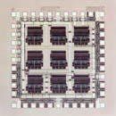
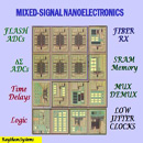
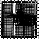
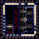
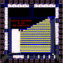
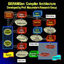
Sample VLSI Chips and CAD Tools 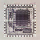

|