EECS 270: Introduction to Altera DE2 and Quartus CAD tools
rev 8/17/10Acknowledgements:
Overview
EECS 270 introduces you to the exciting world of digital logic design. Digital devices have proliferated in the last quarter century and have become essential in just about anything we do or depend on in a modern society. Computers of all varieties are now at the heart of commerce, communications, education, health care, entertainment, defense, etc. Personal computers have become standard fixtures in most homes and even in preschools. But while the computer is the most visible digital computing device, it is by no means the only one. Embedded (invisible) digital controllers can be found in such diverse applications as automobiles, airplanes, elevators, cellphones, televisions, cameras, and many kitchen appliances, to name just a tiny few. We are in the midst of a digital revolution that is transforming our way of life in ways far more profound than any other technological invention in the history of mankind. It is breathtaking.
This course provides you with a basic understanding of what digital devices are, how they operate, and how they can be designed to perform useful functions. It forms a foundation for the more advanced hardware courses in our curriculum. You will learn about digital design through a combination of lectures, homework, and a hands-on laboratory. The laboratory is an integral part of the course that shows how the theory of digital design learned in lectures is applied in practice to construct real digital systems. This overview document describes the equipment you will be using in the lab, the lab procedures, and a schedule of the experiments you will be performing throughout the semester.
Getting started...
Be sure to attend the first lab. You will be introduced to the hardware kit, CAD software (Quartus Tools) and perform an introductory tutorial.
If you wish to get started before the first lab meeting, you can go to a CAEN lab and run the 270 lab tutorial except for the part that requires the kits used in the lab. The software runs under Linux in CAEN labs and the 270 lab. See the tutorial for more specifics on getting started with the CAD software.
You can also download a web pack version of the CAD software that runs under Windows. Although the web pack version runs under Windows, the project files are compatible with the CAEN and 270 lab software running under Linux. See the lab webpage for current links to free Quartus software.
Altera also provides a great tutorial on getting started with the Quartus Tools. Browse the Altera website for current tutorials.
No support will be available until the first lab meeting, so save your questions until then.
Once over lightly
- Understand the required functionality of the design by reading and interpreting a set of English language specifications. These specifications are typically given to you by your customers; in your case, your customers are your EECS 270 instructors who will give you written specifications for each design in this lab. In general our lab specifications will be more detailed and technical than real-world specifications would be.
- Apply your knowledge of how to design digital systems (which you
will
hopefully acquire this semester) to translate your understanding of the
required functionality into a "paper" design. You will be using special
design automation software to help you with the mundane aspects of the
design process and to let you focus your creative energies on the more
challenging aspects. This design paradigm is commonly referred to as
Computer-Aided Design (CAD for short) and the software programs used to
assist you with design are frequently called CAD tools.
- In this lab you will be using the Quartus II CAD software. It is available in the 270 lab, on the CAEN computers (in Linux) and can be downloaded from the vendor. This software allows you to enter your design and to verify it by simulation to make sure it is actually behaving as required by the specifications. If you detect errors, you should modify it at that point and re-simulate it.
- Implement the design by downloading it to the logic board attached to your lab computer. The main component on this logic board is an Altera field-programmable gate array (FPGA) integrated circuit (IC) chip consisting of many thousands of logic building blocks that can be "wired" according to the pattern of your specific design by appropriately opening and closing tiny electronic switches. The miracle of software hides all of this detail; seconds after you issue the command to download your design, the FPGA becomes the hardware embodiment of that design.
- "Play" with your design. The logic board contains a variety of switches (for input) and indicators (for output) to help you apply stimuli to and observe responses from the FPGA.
The hardware
| You will build several digital circuits this semester,
ranging from a simple function of inputs to something as complex as a
computer or controller interface. Altera's DE2 board is the vehicle you
will use to implement these circuits.
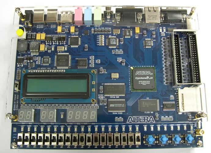
The DE2 (shown on the right; click to expand) is designed to support a wide range of experiments. It combines a variety of logic and I/O devices onto a single printed-circuit board and allows you to configure and control these devices to create different applications. The logic devices on the DE2 are an FPGA (a programmable logic device) and several memory components (SDRAM, SRAM, and flash RAM). The I/O devices on the DE2 are a small LCD display, numerous LEDs (lights), and switches. In addition, the DE2 has connections to a variety of external I/O devices, including PS/2 (keyboard and mouse), USB, VGA (video), audio (microphone and speaker), TV, Ethernet, RS-232 (serial port), Secure Digital and IrDA (infrared). The DE2 board hosts a Cyclone II FPGA with over 33,000 logic elements. In addition it has an LCD panel, eight 7-segment displays, and a host of switches and LEDs, not to mention VGA and audio outputs. |
 |
The software
- Design Entry
There are basically two methods for capturing a design: a) by drawing a schematic diagram showing the design's components and how they are interconnected; and b) by writing a text document that describes the structure and behavior of the design in some appropriate notation. We will use both methods of design entry in this course.The schematic editor allows you to create your design by instantiating components from one or more libraries and by wiring them together. The types of components we will be using ranges from simple logic gates (in the first few labs) to more complex building blocks (such as arithmetic units and data steering logic.) You can accomplish the same task by using the an HDL. HDL stands for Hardware Description Language. These languages are analogous to the programming languages used to write general-purpose software, but are usually augmented with features tures geared specifically for describing hardware. The Cyclone II Tools support two such languages: Verilog and VHDL. These languages two have powerful constructs that essential when you're designing complex hardware; they are the primary HDLs used logic designers in the semiconductor and computer industries. Most EECS classes in the University that use and HDL use Verilog (EECS 373, 470, 427, 627) and so that is the HDL you will be exposed to here.
- Functional Simulation
One of the advantages of computer-aided design is that you can check out the correctness of your design before implementing it in hardware. Basically, you "exercise" your software model of the design (the schematic or HDL description) by applying various inputs to it and observing the resulting outputs. This process is referred to as simulating your design. You can use simulators to check many aspects of your design. For digital design, the two most common classes of simulators are a) functional simulators for checking the logical correctness of the design, and b) timing simulators for verifying that the design works at the required speed. We will focus almost exclusively on verifying functionality, and only briefly explore timing simulation to get some appreciation of the temporal behavior of logic circuits.The Quartus tools provide a functional logic simulator that can be invoked after a design has been entered. The simulator allows you to define stimulators that you can apply to the inputs of your design, and to observe the resulting logic waveforms on the outputs. Any anomalies detected in this process should be diagnosed to determine their cause, and the design should be modified to eliminate them (by switching back to either the Schematic or HDL Editors). When you are satisfied that your design behaves according to its specification, you can move to the implementation stage.
- Implementation
Implementing a design in hardware takes different routes depending on the nature of that hardware. The choices range from off-the-shelf IC chips that must be physically wired together, to custom-designed ICs that are manufactured in a semiconductor fabrication facility, to a whole range of programmable ICs with varying degrees of flexibility. In this lab, the primary implementation medium is the Cyclone II FPGA IC chip; for some experiments we may also interface to other external devices.An FPGA can be programmed to implement a particular design by downloading to it a "configuration" file that tells it how to set the state (on or off) of tiny electronic switches (transistors) so that the structure and function of the chip match those of the given design. The process of generating this configuration file for a given design is quite involved, but that need not concern us here; the Foundation tools conveniently take care of this. What we do need to know is that the resulting configuration file is a binary file with a ".sof" extension; it is also called an "SRAM object file" or sometimes a "bit file".
- Programming
The actional programming of the FPGA involves downloading the "sof" file from the PC to the FPGA. This is done by using the "In-system Memory Content Editor", which is simply a tool to program the FPGA. - Debugging
At this point you will have a "live" design on the logic board and you are ready to check it by applying the various inputs from the switches and other sources and watching the various outputs. While it should work the same as it did in simulation, there are often bugs which only show up in a live design. (For example you are turning on-and-off the wrong LED.) In later labs you may have gitches or other logical errors which only are obvious in a live design.
What we need from you
- Pre-Lab Requirements
The Pre-Lab as the name
implies generally consists of the preparation work for the lab in
question. For most labs this consists of a design and simulation. There
may be some questions to answer that provide some insight into the lab.
The assignments typically require you to submit a design in the form of
a schematic file or HDL file, a pin assignment file, a waveform
simulation file and answers to questions when required. Generally, you
can do the Pre-Lab without the lab equipment or the use of the lab. The
Quartus software is available in the CAEN labs and a free version is
available form Altera. Attend your home lab or open labs for support. - In-Lab Requirements
During lab periods, you are expected to complete the hardware portion of the experiment. For most experiments this means merely downloading your design bitstream file to the logic board; for some experiments, you may also need to wire some additional chips on the breadboard. In either case, you must demonstrate the operation of the circuit to your lab GSI. If the circuit is not behaving according to the given specifications, you are expected to diagnose the causes of the erroneous behavior and to make appropriate design modifications. Your in-lab work is considered to be incomplete until your lab GSI certifies the correct operation of your circuit. This part of the lab obviously requires working in the lab.
- Post-Lab Requirements
Typically this consists of answers to questions. Some labs require additional simulations or other more general questions that require a bit more then a short answer. You do not have to submit design files like schematics, etc if they are the identical to your Pre-Lab files. This part of the lab can be completed outside the lab.