Quartus Software Tutorial

Developed for Quartus EECS 270 at the University of Michigan
By Mark Brehob and Matt Smith, adapted from work by Michael Kontz and Peter Chen.
revised 9/19/15

  1. Purpose
  2. This tutorial steps the reader through using the Quartus II software to implement a simple logic design. It is the author's hope that after reading this tutorial the reader will be able to independently implement their own simple design such as Lab 1.

    Note: This tutorial is for the Linux toolset. The directions likely apply to the Windows version also, but have not been tested there. In lab we expect you to use the Linux toolset.

  3. Example Design Problem - Majority Voter
  4. A majority voter has three 1-bit inputs (A,B,C) and one 1-bit output (M) as seen in Figure 1. The output M takes on the majority value of the three inputs. The truth table shown in Table 1 fully illustrates its function. Whenever two or more inputs are '0' then the output M is '0'. Whenever two or more inputs are '1' then the output M is '1'.

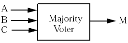
    FIGURE 1: Symbol for Majority Voter


    A B C M
    0 0 0 0
    0 0 1 0
    0 1 0 0
    0 1 1 1
    1 0 0 0
    1 0 1 1
    1 1 0 1
    1 1 1 1

    TABLE 1: Truth Table for Majority Voter

  5. Solution to Design Problem
  6. One solution to the majority voter problem is given in Figure 2. Note that this solution may not be optimal, but it serves the purpose of this tutorial.

    FIGURE 2: Gate Representation of Majority Voter

  7. Quartus Software
  8. The Quartus software used in the 270 lab can also be found in CAEN labs and the Duderstadt Center.
    1. Starting Quartus II

    2. To begin using the Quartus software, first open a terminal window. You can do so by right-clicking on an open part of the screen and selecting "Open Terminal" from the menu. In that terminal window type quartus &. The ampersand tells the terminal window to launch the application "in the background" so that the terminal can be used for other things. It may take a minute for the splash screen to come up, so be patient. If this is the first time you've used Quartus, you will be prompted to select a "view type." Use the default: Quartus II. After a bit you should see an introduction window. Proceed to the next window. It will look something like this screenshot.

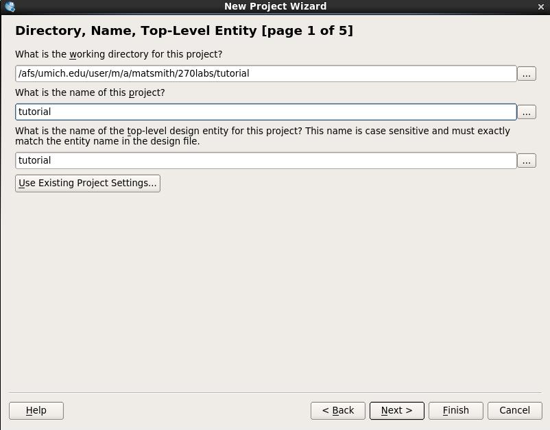
      Click the "Create a New Project (New Project Wizard)" at the splash screen. A screen will appear that has 3 lines of text to fill in. The first line will be populated with the path to your AFS space.  For the directory select any directory name, though we recommend you use something like 270labs/tutorial. For the name of the project and the top level-design entity, use "tutorial". Your window should now look like this screenshot. Select "Next". You should be prompted if you wish to create the directory. Select "yes". You have now created a new project.

      It is best to put each lab or project in it's own directory. For example, when you start lab 1 the path should be 270labs/lab1, lab 2 should be 270labs/lab2, etc.

      Next you will be prompted to add design files. We will create design files a bit later, so skip this window.

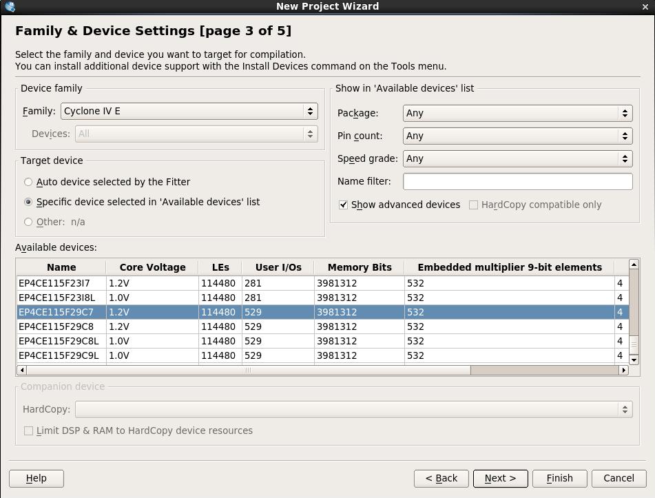
      Now you need to tell the software what type of device you will be using. First select Device Family to be Cyclone IVE. Under Available Devices select EP4CE115F29C7.  If you look on the DE2 board, you will notice that this is the name and device of the Altera chip. The window should look like this.

      Proceed thru the last to windows (4 and 5) and using the default settings.

    3. Design Entry

    4. The first step in creating the Majority Voter is to enter the design into a schematic. To do so, select File → New... from the Menu and then select "Block Diagram/Schematic File" as shown here.

      This will launch the schematic editor. On the left side of the Schematic Editor window is a toolbar containing the different modes of the editor. To change modes, simply click on the appropriate icon. You can also use the "Esc" key to go to the default "Select and Drag" mode. For this tutorial we will be using only the following three modes:

      One common approach to beginning a schematic is to start by placing all inputs on the left and outputs on the right. Inputs and Outputs in Quartus use "pins" (input pins for inputs, output pins for outputs). Since the design calls for three inputs, we will first get three input pins using the "Symbol Tool". Open the "Symbol Tool" by clicking on the "Symbol Tool" icon.

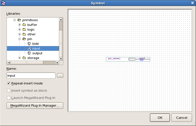
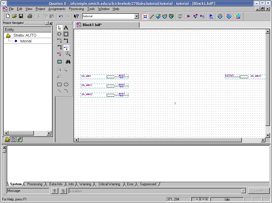
      A pop-up window titled "Symbol" will appear. Click on the "plus" sign under libraries and then on the "primitives" and finally "pin". The Symbol window should now look like this screenshot. Make sure that the "repeat-insert mode" checkbox is selected. Select "input" under pins and press OK. As our circuit has three inputs, place the three input pins on the left side of the screen. Do the same thing again, but placing one output on the right side. Your design should look similar to this screenshot. Note that you can move an existing pin by switching to the selection mode. You can also delete a pin by selecting it and then pressing the "delete" key on the keyboard. You can also return to the selection tool by pressing the "Esc" key on the keyboard.

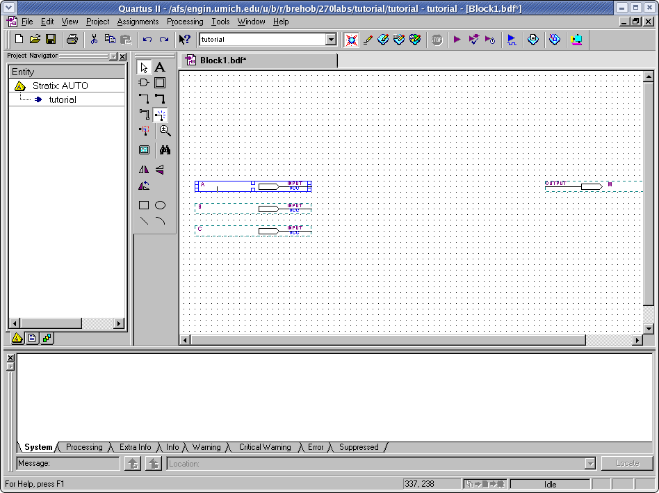
      Next, we wish to give these pins names. Right click on each pin and select "properties" OR double-click on the pin. Change the input names of each of the three inputs to A, B or C. Change the output pin's name to "M". The screen should now resemble this screenshot.

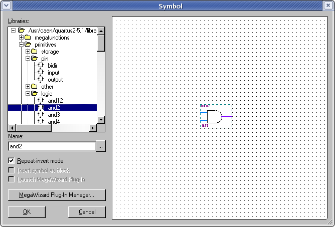
      Now add three 2-input AND gates and two 2-input OR gates. You will want the AND gates in a column to the right of the input pins and the OR gates to the right of them (as seen in Figure 2, above). Don't worry about the wires yet. You can select the gates by using the Symbol tool under "primitives" then "logic". You want "and2" and "or2" (see here for selecting a 2-input AND gate). Once you've added the five gates, your design should resemble this screenshot.

      This would be a good time to save your design. Select File → Save Project and respond in the affirmative to any dialog box which may come up. In general, you should save your work every five minutes or so. We've had a few problems with the tool crashing.

      Next, switch to wiring mode and connect the gates and pins so as to implement the function shown in Figure 2. You may find that the tool doesn't always place the wire in the way you'd like. This can be a real problem when the tool ends up connecting a given wire to things you hadn't intended. A trick is to draw the wire "part way" to where you want it and then end the wire. From that point you can then finish the wire from the other end. This can be a bit tricky and you should ask for help if things don't seem right to you. In general, if you see an "X" at the end of the wire, that means the wire isn't connected at that point. And if a wire touches an input or output, it is connected to that location. You can test for this by dragging a component and making sure the wires move with it. You may find connecting the wires difficult to begin with, and you should be using "undo" (ctrl-Z) as needed to remove mistakes. 
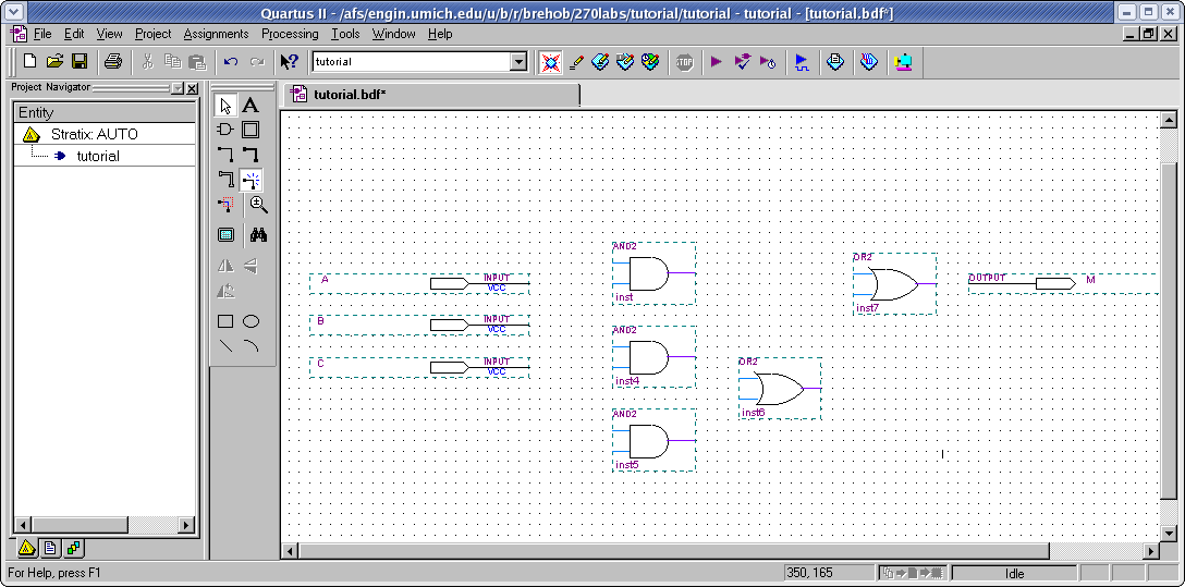
Try your best to draw your circuit so it looks like this:


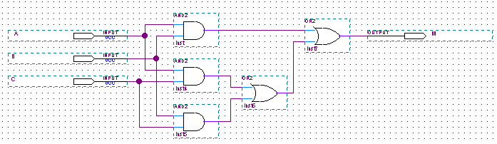
      FIGURE 3: Completed majority gate

      Congratulations, you've drawn your first circuit in Quartus! There is a fair bit more to do, but you've finished the design aspect. At this time it is worth noting that there are other ways to do some of the things we've done. For example, components can also be automatically connected by wires if you place them touching one another and then drag them apart. (If this doesn't work, you should check to see that the "rubberbanding" icon is selected. You can also call up the "Symbol tool" by double-clicking openspace in the design pane (though the repeat-insert mode will not be checked by default).

      To make sure that all wires are connected and none of the components are used incorrectly you can simply pick-up each device and move it around. Its wires should stay connected (again, assuming the "rubberbanding" icon is selected.)

      Again, this would be a good time to save the project. Quartus seems to crash every now and again. So save early and often.

      Your lab assignments will require you to submit an image of your schematic. To create a PDF of your schematic select, File-->Print, and then Print to File (PDF). You can also select the directory path in this window.

    5. Simulation

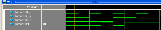
    6. Now that the Majority Voter is completely laid out, we will test its correct functionality by observing the output M when the inputs A, B, and C are given certain values. With the Quartus toolset you can provide a set of inputs to your design and check to see what outputs are generated. This is helpful in finding errors in your design.

      You might imagine the best way to test our design is to provide all the input combinations in Table 1. One way to do this is with a hardware descripton language (HDL) called Verilog. The file and specification is commonly refered to as a test bench. An example of a test bench for the majority voter that tests for all the combinations in table 1 follows.

// means a comment follows
`timescale 1 ns/1 ns //time scale for the test bench


module tutorialtb(); // the test bench module

reg A_s, B_s, C_s; //define input ports
wire M_s; //define output port

// the following creates (instantiates) your majority voter module (tutorial), creates an intance of it (t1)
//and passes the inputs from the test procedure below
tutorial t1(.A(A_s), .B(B_s),.C( C_s),.M(M_s));

//what follows is the test procedure
initial begin

//test all possible input conditions
//#10 means wait 10 time scale units (defined to be ns above)
A_s <= 0; B_s <= 0; C_s <=0; #10;
A_s <= 1; B_s <= 0; C_s <=0; #10;
A_s <= 0; B_s <= 1; C_s <=0; #10;
A_s <= 1; B_s <= 1; C_s <=0; #10;
A_s <= 0; B_s <= 0; C_s <=1; #10;
A_s <= 1; B_s <= 0; C_s <=1; #10;
A_s <= 0; B_s <= 1; C_s <=1; #10;
A_s <= 1; B_s <= 1; C_s <=1; #10;

end
endmodule

      The test bench basically tests your design with a test procedure. You can think of your majority voter schematic as a module having 3 input ports A, B and C and one output port M. We could define a functional reference to the voter as tutorial (A, B, C, M). You might imagine a test procedure that sets the values of a row of the truth table to the inputs, waits a bit so you can see the output, and then sets the next row until all the combinations are tried. This can be done with a Verilog initial procedure. It simply sets values to the test inputs with a delay specified for each case. In this test #10 specifies a delay of 10ns. Next, we must connect the test variables to the majority voter logic in the "tutorial" top-level module. Let's look at the case of port A. The .A part references the port A defined in your schematic. The A_s part references your variable in the test bench. Together .A(A_S) completes the connection. This notation is order independent. For example, the connections could have been listed in opposite order: tutorial t1(.M(M_s), .C(C_s), .B(B_s), .A(A_s)).

      Let's create the test bench file. In the Quartus project manager select  File-->new-->Design Files-->Verilog HDL File to create a new Verilog file. Copy the test bench above and paste into a Verilog file. Save the file as tutorialtb.v. Notice the icon with a check mark in the tool bar just above the open file window. Clicking this will perform a syntax check on your file. It should be ok. Try removing, say, one of the semicolons in the test procedure, save the file, and check again. The error report should give you line specific error information. Fix the error, check it, and save it.

      Quartus uses a common industry simulation tool known as ModelSim for simulation testing. While ModelSim can be run independently of Quartus, Quartus and ModelSim have collaborated to provide a version that can be invoked from Quartus. The advantage is Quartus will pass all the design, simulation and library files that ModelSim needs, but some setup is required in Quartus first.

      First, you must tell Quartus that you wish to use the ModelSim-Altera simulation tool. Go to Assignments → Settings → EDA Tool Settings → Simulation, and in the Tool name window select ModelSim-Altera. In the "Format for output netlist" window, select Verilog HDL. In the time scale window select 1 ns. The output directory should be simulation/modelsim. Keep this window open; there is more to do.

      Next, you must provide Quartus with your test bench module name (tutorialtb) and the location and name of the file. To do this, select the "Compile test bench:" settings (under NativeLink settings) and click on the "Test Benches..." button. A window will open, click New. In the "Test bench name" field, enter "tutorialtb". The "Top level module in test bench" field will automatically fill. In the "test bench files" field, browse for your file tutorialtb.v and add it to the list. Keep all the other settings as they are. Click OK, saving the windows. Your settings window should now look like this:

no image
ModelSim Tool Settings

      Finally, select the "More EDA Netlist Writer Settings..." button and change the "Generate netlist for functional simulation only" setting to On. This specifies that you are performing a functional simulation. Click OK for both windows.

      One last step before we actually run ModelSim. We must check to see if the link to the ModelSim executable is setup. Under tools-->Options you should see the following screen with the path shown in the ModelSim-Altera field. If not, enter the path shown below.

      With these settings in place, you must run a compilation to generate all the necessary files. Select Processing → Start Compilation, or click the purple "Start Compilation" button on the toolbar. The compilation should finish successfully. Invistigate any warnings, critical warnings, or errors.

      If this completes without errors, you can invoke ModelSim by selecting Tools → Run Simulation Tool → EDA Gate Level Simulation. If there are no errors in your design, ModelSim will open. If you see errors in the ModelSim console window, you will have to go back and fix your design or test bench file (expand the ModelSim console to view all the information about the error). If all goes well, you should see a simulation window with your input and output ports and a simulation waveform. Click on the waveform window and a yellow cursor will appear. Zoom in by clicking on the blue "Zoom Full" magnification button to see the entire simulation. The simulation should look something like this:
no image
Majority Voter Functional Simulaton


  A quick reference is provided here Modelsim-Altera Simulation Referece. The simulation guide is linked on the lab webpage for your convenience.
    1. Implementation
    2. Now that your design for a Majority Voter has proven correct, the next step is to implement the design on the Altera board. The first thing you'll need to do is tell Quartus which pin you want to drive each input and output. This will be a file with the qsf file extension, most likely "tutorial.qsf". You can edit this file in Quartus. Open this file under File → Open. Select "all files" and browse for the qsf file. Add the following lines at the bottom of the qsf file:
	  set_location_assignment PIN_AB28 -to A
 set_location_assignment PIN_AC28 -to B
set_location_assignment PIN_AC27 -to C
set_location_assignment PIN_G19 -to M
Note: Editing the qsf file outside of the Quartus application with a text editor may not work. It is better to edit within Quartus.

The set_location_assignment statements associate the FPGA pins with net names in the top level schematic. For example, the first line associates PIN_N25 to net name A. Since PIN_AB28 is connected to slide switch 0, net name A in your schematic will be connected to this switch. Note that it is important to have the correct FGPA device selected for the project, or else a pin error will be generated during compilation. This is because the pins are unique for each type of FPGA. Since the simulator does not depend on correct pin assignments, this problem will not be revealed during simulation.
      In this tutorial we have provided you with the pin assignments. In future labs, you will have to provide the pins and associated IO such as switches and LEDs. The complete pin listing for all the DE2 IO devices is provided on the lab web page under the commonly used files heading as DE2_115.qsf.  Unfortunately, it is not possible to include this file with each project. Instead, you can only include the IO devices you are using for a particular project. Each time you start a project a qsf file is created with out any pin listings. In the case of the tutorial project, tutorial.qsf was created. Typically you will open the DE2_115.qsf file from your browser and copy the relevant pin/device assignments into your project tutorial. Be sure to leave the existing lines in the file adding the pin assignments at the bottom. In this case, we would have selected the following lines from the DE2_115.qsf file.
	  set_location_assignment PIN_AB28 -to SW[0]
set_location_assignment PIN_AC28 -to SW[1]
set_location_assignment PIN_AC27 -to SW[2]
set_location_assignment PIN_G19 -to LEDR[0]

Notice the names associated with pins in the DE2_115 file are generalized. In this case, SW[0] means slide switch 0. If you look at the row of switches running along the bottom of the kit, will see switches labeled SW0, SW1, etc. SW0 corresponds to SW[0]. We changed the name SW[0] to A because it must correspond to the name used in your design file. 

      Compile Design

      Now, compile your project again to incorporate your new location assignments. Simply click this  button in Quartus tool bar.


      You may see a few warnings regarding no clocks found in the design and a few others as shown below. These can be safely ignored.

      Load the Design to Kit 

      Next, you can download the synthesized circuit to the FPGA via the USB cable that connects the DE2 to the computer that is running Quartus.

      First, turn on the DE2 (if it's not already on) by pressing the big red button on the upper left. This should light up the blue power LED (upper left).

      No open the programer by clicking on this button  in the toolbar. 

      The following window will open.


      Click the Add File button and browse to the output_files directory 
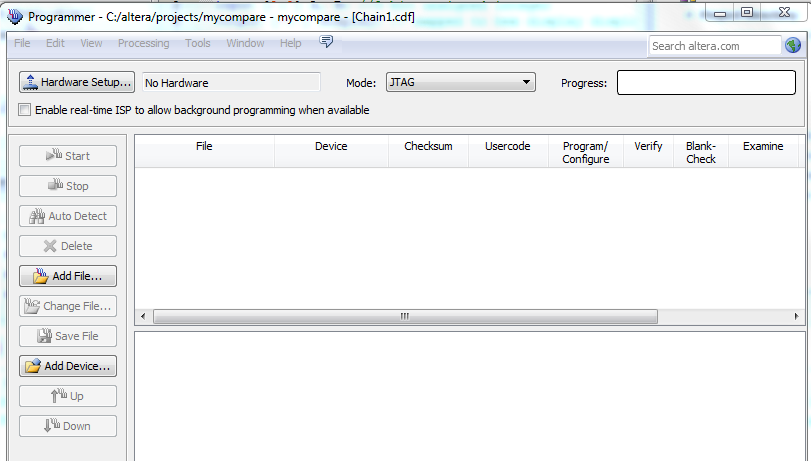
. You should know see a tutorial.sof file. Select this and the following screen should open.
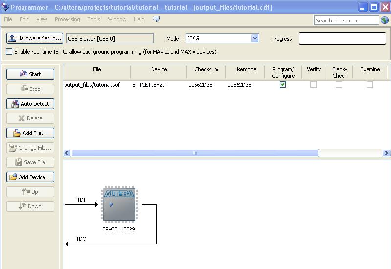

      The tutorial.sof file is the programming file. Select this line and click start. You should see an indicator in the progress window. 

      If a "no hardware" message is shown in the box in the upper left instead of USB-Blaster. Select the Hardware Setup button, choose USB blaster and save. The kit has to be turned on and the USB cable connected from the kit to the computer for the device to be detected. 


    Congratulations! You are now ready to test your design using dip switches 0, 1 and 2 and LED 0. It should work just like in the simulator, making the LED reflect the majority value of the dip switches. Good luck with Lab1!

    Brief Summary of stuff to do when making a project

    1. Use the New Project Wizard to create the project. Use a different directory for each project (Say 270labs/lab1, 270labs/lab2, etc.)
    2. The device settings are: family  "Cyclone IV" and type "EP4CE115F29C7".
    3. The pin assignments are listed in the DE2_115.qsf file posted on the lab page. Copy and paste pin assignments into the project qsf file as needed. 
    4. Create and save your schematic.
    5. Write test benches based on the provided tutorial model.
    6. Make sure simulation settings are specified as above.
    7. For a quick link that summarizes the simulation tool set up, see Simulation Quick Reference Guide

Assignment Submission

There is nothing due for this tutorial lab. The remaining lab assignments will require that you submit a consolidated PDF file via Ctools, which typically consists of schematics, constraint pin listings, answers to questions and simulation waveforms. See the following link for suggestions and submission policy. Lab Submission Policy