EECS 270: Lab 1
Introduction to the Quartus
Toolset
See lab schedule for due dates.
Total Value: 50 points
Revised 12/27/16
- Overview
The main goal of this first experiment is to familiarize you with the
lab
setup and to give you your first formal exposure to the Altera software
and
the DE2 programmable logic board. You will perform all of the design
stages
outlined in the EECS 270 Laboratory Overview.
- Preparation
This being your first lab, the actual design work required is quite
minimal.
However, you need to do quite a bit of reading in order to make this a
useful exercise. Read the following before you do the lab, and refer to
it
as needed later:
- The EECS 270 Laboratory Overview document. This is a good
starting point and a useful reference for data that you'll frequently
need.
- The tutorial we've prepared for
you.
- The post-lab questions assume you know a bit about hexadecimal
notation. Read the supplement included with this lab on hex notation
and number systems.
- Design Specification
The top-level schematic of the circuit you need to design is shown in
Figure 1. Named SELECTOR, it has two 8-bit inputs connected to two
different banks of dip switches (SW7-0 and SW17-10). It also has an
input connected to the KEY3 push-button (leftmost blue button on the
board). It has an 8-bit output connected to the red LEDs 0 to 7, and a
7-bit output connected to the rightmost 7-segment display (HEX0 on the
board). Locate all of these inputs and outputs on the DE2 board before
you continue.
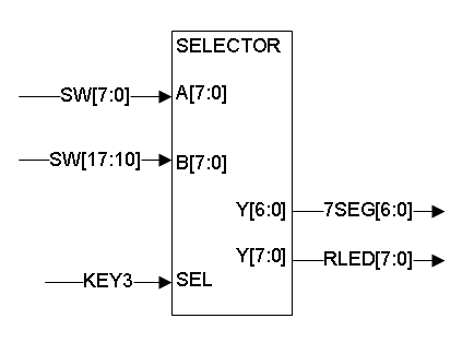
Figure 1: Top-level view of SELECTOR
Your design should achieve the following:
- When the push-button is pressed, the 8-bit word specified by
the settings of the SW[7:0] should be displayed on both the red LEDs
and the 7-segment display.
- When the push-button is not pressed, the 8-bit word on
SW[17:10] should be displayed on both the red LEDs and the 7-segment
display. Since there are only 7 segments, you may ignore the last bit
to be mapped.
- You
are to name your output pins for the HEX0 display H0
through H6. To do this, you will need to append lines to the *.qsf
file. (Hint: copy the relevant lines from the DE2_115.qsf file,
found on the lab web page and make changes as needed.) You may
name the red LEDs as you wish.
The red LEDs should be illuminated so that setting the rightmost switch
of group SW7-0 or SW17-10 illuminates the rightmost LED. In the same
way, the rightmost switch of either switch group should illuminate
segment 0 of HEX0 (see figure 2, below).
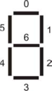
Figure 2: 7-segment display segment numbers
Implementation details
There are two more things you need to know before you can start.
1) Even though we have yet to study
multiplexers in detail, it is
not too hard to realize the functionality of SELECTOR with a pair of
74x157 4-bit 2-way multiplexers. This component is available as a
library primitive that can be instantiated in the Schematic Editor (In
the symbol tool/device library as: others → maxplus2 →
74157).
It has two sets of 4-bit inputs (labeled A1-A4 and B1-B4), a 4-bit
output (Y1-Y4), a select input S, and an active-low enable input
GN.
if(GN==0) Y = 0
else if (SEL == 1) Y[i]=B[i]
else Y[i] = A[i]
2) The HEX outputs are active low.
That means that the
light comes on when a 0 (low) is driven to it. You'll need to think
about how to handle that.
The push-buttons (e.g. KEY3) are also active low. This means that the
pressed state of the button corresponds to 0 (low) and the unpressed
state is 1 (high). This is the opposite of active high input devices,
such as the dipswitches.
See section 2.9 (page 79) of Vahid for a little background on
the mux.
- Design Notes and Hints
- Despite the fact that the top-level schematic is drawn using
buses, you don't have to use busses in your design; simply use
single-bit wires. We'll have plenty of practice with buses later on.
- A logical 0 is represented as the symbol associated with GND. A
logical 1 is represented as the symbol associated with VCC. GND and VCC
are available in the device library under primitives → others.
- Deliverable
-
Pre-Lab (0 points) There is not pre-lab for this lab.
- In-Lab (15 points)
Generate the .sof file for SELECTOR, download it to the board,
and verify that your implementation is working properly. When you are
satisfied that you have a correctly- functioning circuit, print the
In-Lab certification sheet and demonstrate its operation to a 270 lab
instructor. The instructor will collect the demo sheet.
- Post-Lab Questions (20 points)
Submit answers to the following questions.
- Consider a MUX which has a single control line (C) which
selects between two inputs (A and B) to generate one output (M). Draw a
truth-table for this device. Assume the input A is selected if C=0,
otherwise the input B is selected. (5 points)
- If you were to construct a truth table for SELECTOR, how
many rows would it have? How many (input and output) columns? (5
points)
- Assuming that SW[7..0] = 0x5E and SW[17..10] = 0x97 (these
are hexadecimal values), which red LEDs remain lit regardless of
whether the button is pushed or not? (4 points)
- Assuming Key3 is 1, which switches must be set to what values
if you want a "7" to be displayed on the seven-segment display? What if
you wanted a "1" and Key3 was 0? If a given input doesn't matter, don't
list it as part of your answer. (6 points)
- Post Lab Simulation (15 points)
- Submit the SELECTOR schematic and .qsf listing. (10
points)
- Submit the SELECTOR's simulation waveform and
test bench showing its response on the appropriate
7-segment display and LED outputs to all possible combinations of SW0,
SW10 and KEY3. inputs. You must implement the following truth table for
your test procedure. (5 points)
KEY3 SW0 SW10
0 0
0
0 0 1
0 1 0
0 1
1
1 0 0
1 0 1
1 1
0
1 1
1
Take a look at the majority voter tutorial for review on test benches
and using the simulator. The following is an example testbench that you
can modify for this lab. (5 points)
`timescale 1 ns/1 ns
module lab1tb();
reg SEL_s, A_s, B_s; //define input ports
wire Y_s, YY_s; //define output port
//this part connects the test procedure to your
schematic
//the port names will depend on the port names
(IO connectors) you used in your schematic
//H is used for 7SEG since leading with a number
is usually a bad idea
lab1 t1(.SWA0(A_s), .SWB0(B_s),.SEL(
SEL_s),.RLED0(Y_s), .H0(YY_s));
//the test procedure
initial begin
A_s <= 0; B_s <= 0;
SEL_s <=0; #10;
A_s <= 1; B_s <= 0; SEL_s <=0; #10;
A_s <= 0; B_s <= 1; SEL_s <=0; #10;
A_s <= 1; B_s <= 1; SEL_s <=0; #10;
A_s <= 0; B_s <= 0; SEL_s <=1; #10;
A_s <= 1; B_s <= 0; SEL_s <=1; #10;
A_s <= 0; B_s <= 1; SEL_s <=1; #10;
A_s <= 1; B_s <= 1; SEL_s <=1; #10;
end
endmodule