| Home |
| High Level Design |
| Hardware Design |
| Software Design |
| Project Result |
Hardware design
(diagram 2 serial data scheduler macro design) (diagram 3 mpc823 lcd controller)
Serial data communication
The Nintendo gamecube controller uses 64-bits serial data protocol. The console requests data from the controller by sending a 24-bits data pulses, and waits for the controller to respond wit the 64-bits data that contain the controller status.
The 24 bits sent to the controller is as follow: 0100 0000 0000 0011 0000 0010
The 64-bits data bounced by the controller is mapped as follow:
Byte 0 0 0 0 Start Y X B A
Byte 1 1 L R Z Up Down Right Left
Byte 2 Joystick X Value (8 bit) (Analog -> Digital)
Byte 3 Joystick Y Value (8 bit) (Analog -> Digital)
Byte 4 C-Stick X Value (8 bit) (Analog -> Digital)
Byte 5 C-Stick Y Value (8 bit) (Analog -> Digital)
Byte 6 Left Button Value (8 bit) (Analog -> Digital)
Byte 7 Right Button Value (8 bit) (Analog -> Digital)
Note : Each data bit (either 0 or 1) is represented by a sequence of 4 bits data,
1 microsencond each. A 0' is represented by 0001' and a 1' is represented by 0111', each of which takes 4 microsenconds. This is true for both direction of data transfer.
Every data transfer is terminated by a stop bit ( a 1' at the end of the data)
(* all data thanks to James Ward < j.w.ward@dcs.hull.ac.uk >, who made our life easier)
The Nintendo gamecube controller has 12 digital inputs, and 3 analog input devices. The digital input devices are buttons: Start, Y, X, B, A, L, R, Z, Up, Down, Right, Left. (*the digital L and R are active when the L and R buttons clicks'). The analog inputs are the 2 joysticks (the gray and yellow), the Left and Right button(no clicks). Each of the joysticks values are represented by the X and Y position, each of which is defined by 8 bits values. When the X is tilted to the left, the byte value is < 8'b10000000, and when X is tilted to the right, the byte value is > 8'b10000000. There seems to be some percentace of error as the normal' position of the joysticks are not exactly 8'b10000000.
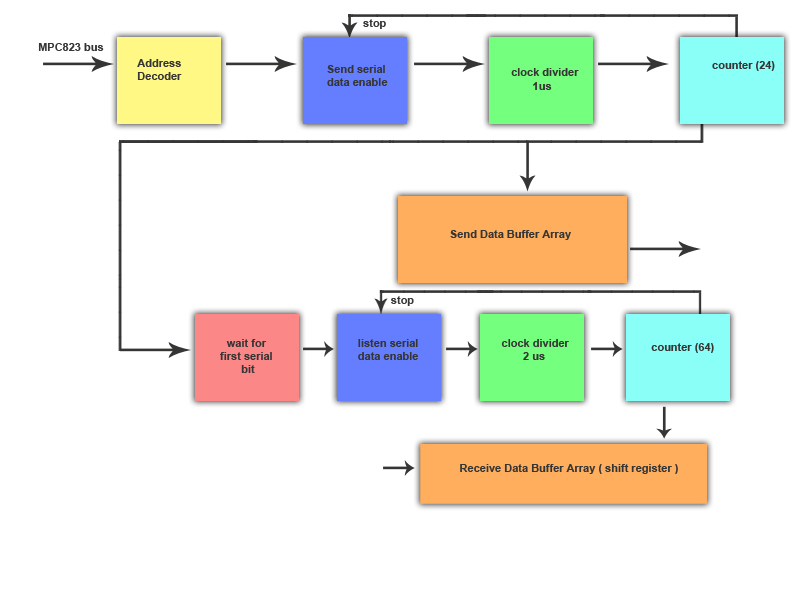
Our serial data scheduler is responsible to trigger the start of sending and requesting data from the controller and is implemented as hardware in the FPGA. The processor will write data to address 0x0290000 on the bus and the macro will trigger the sending the 24-bits of data to the controller, then hold the line high when its done. Total time to send serial data is (24+1)*4 micro seconds = 100 microseconds. The marcro would also assert transfer acknowledge to the processor immediately (1 cycle after transaction start), and assume that the processor will not be requesting data anytime before 360 microseconds after starting serial communication.
After which, the macro will keep watch of any falling edge on the data line that is caused by the controller. A falling edge detected any time after the console is done sending data indicates that the controller have started sending data. The macro will start putting the data into shift register after that.
The start' of each bit is marked with a falling edge of the data line, since both the sequence that represents either 0' and 1' starts with a 0 and ends with a 1. Thus, the actual data is represented by the second and third bit sent by the 0001' or 0111' sequence. Thus, actual data measurement is triggered every ~2 microseconds after the falling edge of the serial data line.
Upon completion of the serial data transfer from the controller to the module, there are 2 ways to interrupt the processor to notify it about the data from the controller is ready at the module. One way is by using edge triggered interrupt at either IRQ1 or IRQ7, while the other way is by using a timer interrupt that triggers at certain time that allows the serial request and serial data receive to complete. Both interrupt ISRs reads from the location 0x02900000 to get the data from the macro. We chose to use the latter method as we find it more convenient to request the status of the controller at evenly distributed time, so that the game will run at constant beat.
To create an exact timing for the serial data triggers, we have to create our own clock dividers. The first clock divider was needed to send the data to the controller to request for controller's status. This clock triggers every ~1 microsecond. The second clock divider that we created was to receive data from the controller. The clock should trigger 2 microseconds after a falling edge in the serial data line is detected, and no triggers after that, unless the counter is reset to 0. When a falling edge is detected, the clock divider counter is then reset to 0 again, so it will trigger 2 microseconds after.
LCD Controller
The MPC823 controller is initialized by the core, which provides the frame buffer address, operational modes, and various configuration bits that the LCD controller needs to operate. The lcd controller uses DMA to fetch frame buffer data, thus is transparent to the processor's activities. The DMA functionality fetches display memory into the FIFO for pixel generation.
The configuration of the registers are as follow:
LCFAA: address of the target DMA - 0x00020000
LCVCR: vertical configuration register - 320 lines/frame
LCHCR: horizontal configuration register - 240 pixels
SCCR: System clock configuration register - divide by 8
LCCR: LCD controller configuration register - enable PON bit to enable LCD