EECS 373 Final Project: Guitar Effects Syntehsizer
by Jared Chenkin and Chris Hsiong
| Introduction |
Hardware Design
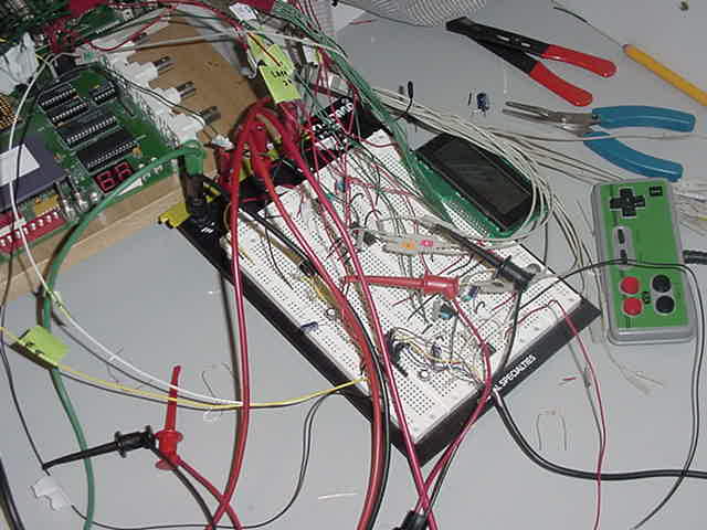
In this project, the hardware served as doing much of the support functions that were necessary for the project to function, but should not or could not have been implemented in software. The hardware dseign did the work that was necessary to keep the software straightforward, understandable, and predictable. The Analog-to-Digital Converter (ADC) that Matt gave us was a Maxim 195BCPE, a 16-bit serial ADC. The first challenge for the hardware was to implement a shift register to capture the data and present it to the data bus all 16 bits at a time so that it could be read and processed as a normal halfword by the software. After dividing the clock down to 1.25 MHz (the maximum clock frequency that the ADC allowed was 1.7), we noticed that the EOC# signal "framed" the data bits. With the ADC that we worked with in class, the only important edge of EOC# was the falling edge, which we used to trigger our interrupt; the rising edge was of no concern. However, with this ADC, the rising edge of EOC# occurre precisely when then first data bit was valid, and successive data bits were presented on rising clock edges. Since we were generating the clock inside of our hardware design, all we needed was two 8-bit serial to parallel shift registers (74x165S) with the clock as the 1.25 MHz clock going to the ADC and the Clock Enable (CE) as EOC#. The serial in for the first SR was the Data bit coming from the ADC, and the last parallel out bit was tied to the serial in on the next SR, creating the 16-bit shift register. Then, when EOC# fell, it would trigger IRQ1, which launched our interrupt service routine (ISR) that grabbed the data off of the outputs to the shift register. We used a read to address 0x3000000 to get the data from our ADC. The trick was that the data was guarenteed to be valid when EOC# fell because, from the ADC's perspective, it was no longer framing the data, and from the hardware's perspective, CE was no longer asserted, so the SR's were no longer shifting any new data bits, but holding the current ones. The last step of the ISR was to write to address 0x3000000, which triggered the START signal for a new conversion to occur, indicating that until the next falling edge of EOC#, the data will not be valid. The next piece of hardware that requires support from our hardware design was the Digital-to-Analog Converter (DAC). We also obtained a DAC from Matt, who gave us a Maxim 541, a 16-bit serial DAC. The DAC worked on a much higher clock of 10 MHz,however we found that the most important aspect of getting the DAC to work properly was meeting all of the timing specifications. The first element needed was a parallel-to-serial Shift Register, and Xilinx did not seem to have one of those, so we built one using 16 D flip-flops and 2-to-1 multiplexors. The SR was clocked off of the 10 MHz clock for the DAC, and was given 16-bits of data from the data bus to shift out one at a time. The S_R signal dictated whether or not the data was being loaded into the 16 flip-flops or being shifted out. The timing for the DAC specified that the Chip Select (CS#) would be held low during the 16 bits that got shfited out. However, this means that the CE for the SR would be held high for at least one additional clock cycle so that the data could get shifted in, and would have to be together with the S_R signal indicating load rather than shift. Additionally, since TS# would come with the faster 20 MHz, for our address decoder, we needed to hold it for twice as long so that it would always be aligned with the same edge of the slower 10 MHz, and not screw up the timing once and a while. In order to get the signals to be held for hte right length at the right time, an SR flip-flop was set when the DAC write command first came in, and was reset after 16 cycles using a binary counter. For the LCD, we used two 4-bit counters (74x163) to count to 6 to get the timing on the Enable and register select signals to match the timing in the specifications. And for the Nintendo 8 controller, we used Verilog to make a finite state machine that generated pulse and latch signals that corresponded to the specifications. Then, to capture the data, we used an 8-bit serial-to-parallel shift register whose output was tied to an 8-bit register. The MSB output of the shift register was then tied to IRQ1, so in the event of a button being pushed, a zero would get shifted though and trigger the interrupt. Then, the ISR would read the register that held the full byte of the buttons' state. |
Hardware Design |
|
| Software Design | |
| Results | |
| Conclusions | |
| Media | |
| Appendix | |
| References |