Home ||| Hardware Design ||| Software Design ||| Media ||| Member Task Distribution ||| High Level Design ||| Results ||| References ||| Conclusion
High Level Design
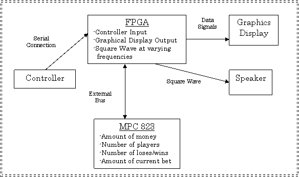
1. To control our three components, we designed the digital logic in different ways.
For the graphics display, there were four commands we needed to implement in order to interact with the display controller: reading the data, writing the data, reading the status of the display, and writing a command to it. To write text, we set a region in the display RAM of the graphics controller for Text (the start of this region and the size of the region), set the number of characters per a column (max of 40 which we used). The location on the screen of each character is mapped to a specific address in the display RAM (for example, the first character of the first line is at Text Home, the second character of the first line is at Text Home + 1, etc.), and will hold some data (a byte) corresponding to an existing character code, or to a user defined character code. For graphics, we also set a region in the display RAM of the graphics controller (the start of this region and the size of this region), the number of pixels per a line (max of 40 which we used). For the graphics, the pixels are written in groups of 6 or 8 (we used groups of 6) using byte writes, so to write the first 6 pixels of the first line to be black, a 0x3F needed to be written the address of the Graphics Home. So each image that we produced consisted of many coordinated byte writes to either the Text Area of the Graphics Area of the display RAM on the Controller. Depending on the display Mode of the controller, the contents of its Graphics and Text regions were shown on the display in some way.
For the Nintendo-8 Controller, two signals controlled it: Latch and Pulse. In order to receive a sequential stream of the data representing the state of the buttons, we needed to send a high signal of 12 microseconds to Latch, then after 6 microseconds, send 8 high pulses each having a 6 microsecond length, and each separated by 6 microseconds.
The Speaker was driven by a square wave, whose frequency is controlled by writing the desired frequency to a data
The graphics display is controlled through assembly language programs that clear out the screen, and then configure the Text and Graphic Regions to the desired patterns. The Nintendo-8 controller is accessed using an assembly program, which reads the input, and incorporates a one-second delay to prevent reading multiple button presses for 1 button press.
2. There are three main components of our design:
3. Functional Block Diagram